
Understanding the concept of PoP (Package-on-Package) technology
Over the past decade the embedded world has undergone tremendous change. With the advent of mobile phones, smart lifestyle gadget like wearables, health and wellness devices, on the consumer front, users are demanding smaller and thinner gadgets.
This has lead in turn to designs that increasingly need efficient memory architectures such as high memory capacity and high performance in small area and multiple bus issues that call for high scalability. The designs demand compact and more densely populated electronic assemblies.
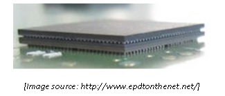
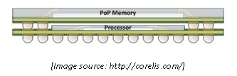
Package on package (PoP) is one of the techniques to address the demand for compact assemblies. PoP is a stacked packaging method to have two ball grid array (BGA) packages mounted one above the other with a standard interface to route signals between them. The most widely used integration components for stacking are the processor and memory. The combination of RAM & Flash memory in single chip BGA solution is also available, which allows a much higher component density on smaller form factor PCB design through the PoP assembly.
Stacking memory is one way to achieve the dual goals for enhanced functionality and greater packaging density of a product. It is fast becoming a promising solution, offering high integration that leads to product miniaturization.
Mobile applications can benefit from the combination of this stacked package, offering small footprint and minimal PCB space. Other portable electronic products such as
• mobile phones (baseband or applications processor plus combo memory),
• digital cameras (image processor plus memory),
• PDAs, portable media players (audio/graphics processor plus memory), gaming and others also benefit from this design approach.
Benefits of PoP Technology
Using PoP technology in a design offers many advantages. The most obvious is the reduction in the PCB size or the small footprint of the PCB. Using PoP technology also ensures a reduction in the no. of layers of the PCB as the connection lines between the processor and the memory are minimized. This also improves signal integrity on the board by minimizing trace length between different interoperating parts, such as controller and memory. The direct interconnections between the circuit yields reduced propagation delay, noise and cross-talk. Using PoP technology also makes for easy memory scalability on the hardware. This is because most of the memory modules for PoP design come in multi-chip packages (eg: Flash + DDR). Hence, both the Flash and DDR memory can be upgraded by replacing the single PoP memory package. And finally, there is the reduction in BoM cost achieve as a result of elimination of termination discretes on the PCB.
The ARM advantage
PoP technology is most popularly being used with ARM Processor Applications. Texas Instruments was one of the first semiconductor companies that adopted this technology. This is now being followed by other silicon vendors like Freescale etc. ARM chipsets are known for low power and are popular for small footprint, portable applications. The low power ensures less thermal radiation to the memory; when it is placed over the processor in the PoP technology. In comparison, Intel SoCs and other DSP are high power and have high thermal radiation. Therefore, there is a possibility of the memory to stall during operation, if the PoP technology concept is used for these chipsets.
An important point to note for product developers is that assembly of PoP PCBs requires special skillset and the need to follow a defined assembly process. The PCB manufacturer should follow the required methodology to ensure minimal yield issues for a successful implementation to take advantage of the benefits of such a design.
*Published in EE Times India