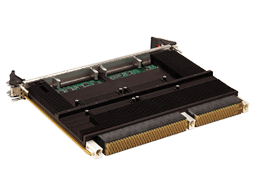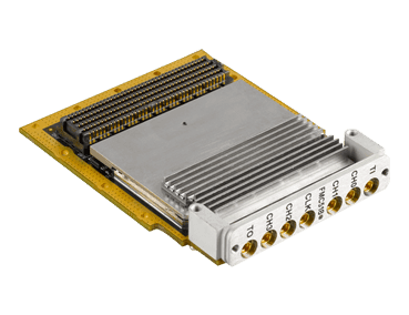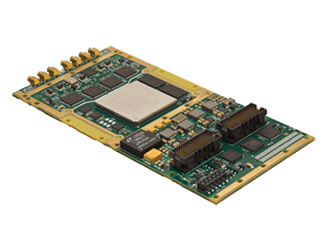

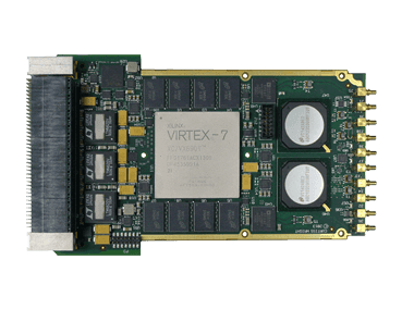
VPX3-530
3U VPX Virtex-7 FPGA rugged dual-channel 4GSPS ADC/DAC is ideal for SWaP constrained platforms such as UAVs, fighter aircraft and ground vehicles.
Overview
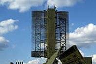
The VPX3-530 is a 3U VPX Virtex-7 FPGA ADC/DAC from Curtiss-Wright that combines multiple channel high-speed ADCs and DACs with a latest generation user programmable Xilinx Virtex-7 FPGA in a vast array of rugged build formats for demanding applications such as RADAR, Electronic Warfare (EW), Signal Intelligence (SIGINT) and Radar Warning Receivers (RWR) applications.
Up to four analog inputs are supported by the VPX3-530. These analog inputs can be configured as dual 4 Gsps/12-bit using native interleaving of the ADC devices or four 2 Gsps/12-bit channels. Each analog input is AC coupled via baluns for maximum ADC performance. The analog inputs are complemented with two 5.6 Gsps 14-bit DACs. Each DAC has a maximum data rate of 2.8 Gsps. Outputs above 2.8 Gsps are achieved through data interpolation modes.
The VPX3-530 features a user-programmable Virtex-7 VX690T FPGA (speed grade 2), a member of Xilinx’s 28nm 7-Series family, that is supported by two high-speed DDR3L memory resources directly connected to the FPGA. The FPGA configuration images can be stored in either the flash memory or DDR SDRAM configuration memory and can be updated by the host CPU using the PCI Express® (PCIe) interface. The DDR DRAM resource supports configurations to be downloaded from the host and bypass the non-volatile flash. Because SDRAM-based configuration is volatile, it is perfect for security-sensitive applications and allows the VPX3-530 to be more easily declassified should the need arise. The FPGA can be reconfigured from any one of many images indexed in the flash including a write-protected recovery configuration. FPGA configuration from either flash or DDR SDRAM can also take advantage of AES encryption.
The 3U VPX Virtex-7 FPGA ADC/DAC, VPX3-530 provides the choice of two (2) RF sample clock sources through the front panel. Modes are supported that allow synchronous ADC and DAC data sampling or independent sample clocks for the ADCs and DACs. This enables coherent input and output sampling or the ability to operate the ADCs and DACs separately. To deliver the maximum performance the VPX3-530 uses an external clock source instead of a local sample clock. A key feature of the VPX3-530 is its ability to operate in a synchronous mode across multiple boards to form an array of synchronized analog inputs. This feature plays a vital role in applications like SIGINT/Direction Finding (DF) or any other applications demanding precise beamforming capabilities.
TECHNICAL SPECIFICATIONS
- Dual 4 Gsps 12-bit or Quad 2 Gsps 12-bit analog inputs
- Dual 5.6 Gsps 14-bit DAC update rate (maximum 2.8 Gsps data rate)
- Multi-board, multi-channel synchronization
- Xilinx user programmable Virtex-7 VX690T FPGA
- Up to 8 Gbytes DDR3L SDRAM (64-bit data paths)
- 3U OpenVPX compliant
- Onboard power and temperature measurement
- VxWorks and Linux host support
- Air- and Conduction-cooled variants
- Applications: Radar, SIGINT/ELINT, Electronic Warfare (EW)