


System Performance Optimization for Embedded Devices
Industrial automation systems typically require data acquisition and processing in real-time. These systems could range from a simple lighting control system to a large distributed control system comprising of sensors/actuators, industrial gateways, monitoring and processing units. Designing such an embedded system puts forth a lot of challenges for design engineers in terms of striking a balance between low-end micro-controllers to performance oriented processors. This can be addressed in an optimal way if the design is done keeping the complete system and its end goals into consideration.
I’ve put forth here a high level approach to overcome these challenges using various system resources to enhance the performance.
The System
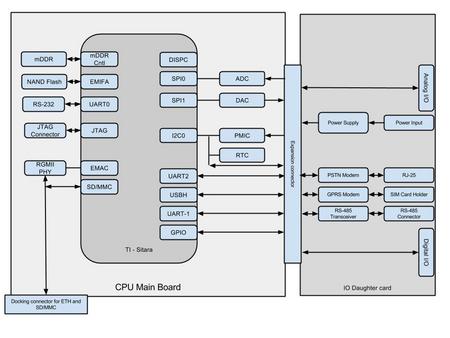
We were designing an industrial data acquisition system and had constraints in terms of the total product cost. We opted to go with a TI-Sitara processor with ADC and DAC connected over the SPI bus. The system also has the Digital IO expander connected over I2C based IO expander. The system runs on Linux Operating system (with RT patch) with standard BSP & Drivers for all on-chip peripherals.
The key aspects of the system are: –
- System running Modbus client responding to the MODBUS master for read/write of system configuration and real-time data
- System running Web-Server to allow the control/configuration of the system and monitoring of real-time parameters
- Capable of handling up to 16 Analog input & 16 digital input.
- ADCs capable of capturing the input signals with the sampling rate of 1 KHz for each channel.
- Digital input being monitored and state changes being responded within 10 milliseconds.
System challenges
The single largest challenge determined during the implementation and testing is associated with the capture of the analog input. To be able to capture the analog input at 1KHz for all channels, the ADC has to be configured for higher sampling rate of 16KHz. Since the ADC does not provide the buffering, all the captured data will have to be read immediately to avoid it being overwritten with new data corresponding to different channel.
The ADC provides an interrupt after completing the conversion for each channel. The standard driver implementation would register the interrupt and initiate the read of the SPI registers. Incidentally, for reading the SPI registers, there is a need to perform SPI register write (so as to generate the required clock). Due to interrupt latencies of Linux (even with the RT patch incorporated), the ADC capture is being missed.
Below is the representative summary of the flow of control and data.
- ADC completes the conversion and asserts the End of Conversion (EoC) signal
- The Sitara registers this EoC line as interrupt and invokes the Linux GPIO Interrupt handler
- The kernel space interrupt handler determines the source to be ADC and then accordingly invokes the ADC drivers
- The ADC driver in kernel space issue an SPI bus read and thus reads the conversion value
- The value is then given to the user’s space application for further processing.
Owing to the large interrupt latencies, context switching time in Linux and the interaction between the kernel space and user’s space components, there was an overall delay. This limits the overall sampling rate.
Systems approach
Issues like the one stated above are likely to occur while various disciplines are working as islands; i.e., the hardware, BSP & applications are working disconnected with each other having fixed interface plans. Instead, if the design is done keeping the complete system and its end goals into consideration, such problems can be solved in much optimal way. This is Illustrated below.
The Sitara is a complex SoC having multiple features including DMA engines. These DMA provide multiple features including event based triggering and chaining. These features have been exploited to solve the above problem. Below is the outline of control and data flow.
- The EoC signal from the ADC is configured to trigger the DMA for issuing the SPI Write (so as to generate the clock). The clock also causes the ADC to transmit the converted data into the SPI lines all the way into the internal receive shift registers of SPI controller in Sitara
- Being full, the internal receive shift register triggers another DMA to read the data from shift register to the memory buffer
- Steps 1 & 2 are repeated for 16 channels. After 16 channels data is transferred to system memory by DMA, the DMA generates transfer completion interrupt
- The interrupt handler transfers the data corresponding to 16 channels and reconfigures the DMA for next transfer waiting for EoC
- The hardware timer is separately configured to generate the required Start of Conversion signal to ensure the sampling interval is deterministic. The ADC is configured to carry out all the channel conversion and stop (waiting for subsequent Start-of-Conversion signal).
This approach yielded the following benefits.
- The system load (CPU Load) is reduced as the Sitara is no longer executing the interrupt handler for every channel conversion completion
- The reliability of the sampling rate is hardware timer controlled and thus immune to variations on the CPU load
- Able to achieve greater sampling rates reliably.
Thus, as showcased above, a thorough understanding of the SoC and its features and seamless integration between the hardware, BSP and application are key to a successful optimization of System performance optimization for a variety of embedded devices.
*Published in EE Times India