
RF Data Acquisition Card for Direct Sampling of L-band to X-band Signals
Overview:
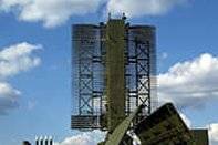
RF Data Acquisition Cards are gaining immense popularity as they are replacing the conventional RF superheterodyne receiver architecture with Direct Sampling Architecture. These boards can directly digitize RF carriers up to X-Band frequencies with an instantaneous bandwidth of 3GHz. The Wide Band Acquisition Cards find a wide variety of applications in Phased Array Radars, Electronic Warfare, Signal Intelligence (SIGINT) Systems, Multi-band Diversity Digital Receivers, Satellite Communication, etc. 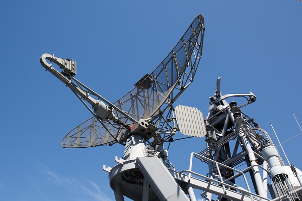
This case study showcases Mistral’s expertise in design and development of a multi-channel data acquisition card, with consists of FPGAs, ADCs, JESD204B compliant clock schemes, etc. that offers unprecedented speed, signal fidelity and on-board real-time data processing – all in the smallest form-factor.
The Customer:
The customer is a leading Defence Research and Development Organization, India. The customer is involved in the research and development of avionics systems for Indian Defence.
Requirement:
The customer approached Mistral to develop a RF Data Acquisition Card (RFDAC) – 6U VPX based conduction-cooled module that adhered to VITA 46 standard, for one of the Avionics projects. The card had to digitize the incoming RF signals at a sampling speed greater than or equal to 6GSps. This was a Build-to-spec project and the preliminary design of the RF Data Acquisition Card was provided by the customer. Mistral had to conduct a feasibility study of the design; and any changes / improvements in the design had to be discussed and finalised with the customer.
The RF Data Acquisition Card development involved:
- Design architecture of the RF Data Acquisition Card.
- Schematic capture as per the final design approved by the Customer
- PCB layout for RFDAC and the test jig [Backplane] – The boards had to meet Group A certification standards and the assembly procedure as per IPC standard
- High-speed signal simulation and analysis.
- Signal integrity, power integrity and thermal analysis
- Fabrication and bare board testing of the fabricated card and assembly as per IPC standard
- Functional testing of the assembled card
- FPGA firmware and software development for all hardware interfaces
- Development of test jig for the RFDAC to test all the peripherals
- Acceptance test procedure for standalone testing of the card with test jig & host PC
- Design & fabrication of a cover Plate [Conduction-cooled heat sink plate] for RFDAC for thermal management and RF shielding
- Wedge lock mechanism to be provided to mount the RF Data Acquisition Card
Solution Provided:
Mistral developed the RF Data Acquisition Card, meeting all the requirements as defined and agreed with the customer. Mistral ensured that the 6U VPX based conduction-cooled module meets all the requirements of VITA46 standard.
The board consists of Eight ADCs to digitize the incoming RF carriers simultaneously. All the ADCs are phase matched and clocked with programmable Sampling clocks. Two high-speed FPGAs acquire and process the data with necessary digital signal processing algorithms. This processed data is sent to other modules in the system using PCI Express interface via VPX backplane. The FPGAs on board are interconnected with each other with a high-speed serial interface for seamless operation. The card is designed with an appropriate power section to provide power for the entire board. All the voltage rails are derived from +12V and +5V DC supplies available on the VPX backplane.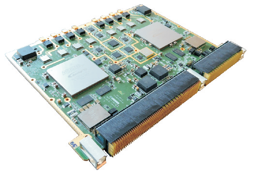
Features:
RF Data Acquisition Card – a conduction cooled 6U VPX Form factor Card – is built around Intel FPGA and TI ADC. The various features of the Card include,
- Dual high speed, high-density Arria-10 FPGAs
- 8 Nos of 12-bit JESD204B compliant ADCs
- Programmable JESD204B compliant clocking section
- 4 lane PCIe connection from each FPGA to VPX backplane
- Gigabit Ethernet, RS232 and RS422 Serial Communication links from each FPGA terminated to backplane connectors
- 2GB of DDR4 per FPGA and 64GB of NAND flash per FPGA for recording acquired data
- Hard Reset Control through firmware or external reset; soft reset through software
- Remote programming of the FPGAs via Gigabit ethernet in addition to JTAG option
- High Speed 4 lane Serdes interconnection between FPGAs
6U VPX Backplane
Mistral custom designed and developed a backplane [Test Jig] to test all the peripherals of the Card. It is a 3-slot 6U VPX backplane designed to test all the interfaces of the RFDAC. Key features of the 6U VPX backplane include,
- 10 Gbps performance
- 2 Nos of PCIe X4 Slot connectors from each VPX slot
- 2 Nos of Ethernet PHY Transceivers with RJ45 connector from each slot
- Interfaces for power, system control, UART, JTAG, geographical addressing, data bus and GPIO connections
Mechanical Cover-plate cum Heat sink
Mistral designed and fabricated a cover-plate required for thermal management and RF shielding of the conduction-cooled RFDAC. The cover-plate is fitted with a wedge lock mounting mechanism.
The cover-plate is designed as below.
- 6U Form factor
- Designed & manufactured custom heat sink plate with the latest available technology
- Operating temperature: -40°C to +71°C
Software & Firmware
BSPs, IPC Libraries & IP Cores
BSP for NIOSII Softcore processor is developed as per the board requirements. BSP, drivers and libraries compatible with VxWorks 6.9 OS.
ATP software
ATP software developed to conduct functional testing of the RFDAC.
FPGA firmware
Mistral provided firmware for all high-speed data acquisition, along with peripheral interface configuration codes.
Test GUI
Mistral developed a test GUI using QT. The GUI is designed to test all peripherals of the card and capture & plot ADC test results. It is connected to the host PC (where GUI is installed) via Ethernet interface on board.
Functional Tests:
Functional tests are done to test and validate the functionality of each component and interface provided in RFDAC. The test procedure includes following checks,
- ADC performance like SNR, SFDR, ENOB etc
- Data acquisition for various sampling rates up to 6Gsps
- Testing of internal interfaces: High-Speed SERDES communication between FPGAs, clock synthesizers programming, DDR4 and Flash read and write, etc.
- Testing of external interfaces: PCI Express interface/ GbE/ RS422/GPIO’s on VPX backplane.
Environmental Stress Screening:
Mistral performed ESS as per MIL-STD-810G. The card was subjected to ESS as per the following tests, specification and sequence.
- Power Burn-in Test
- Pre-thermal Random Vibration
- Thermal Cycling
- Post-Thermal Random Vibration
Read the full case study to know how Mistral overcame the challenges of extremely high heating and complexities of routing high-speed signals.
