NVIDIA Jetson Modules and Use Cases – Part: 2

The first part of the Blog was focused on various NVIDIA Jetson System on Modules and their hardware capabilities. This blog will look at some of the popular use cases of these SoMs. All these use cases come with a perfect balance between power, performance, and energy efficiency which is fundamental to autonomous machines, edge computing and other compute-intensive applications.

Scroll down to know more about various use cases of Jetson Platforms and jumpstart your inventiveness with these powerful SoMs.

NVIDIA Jetson Use Cases

Autonomous Systems and Platforms

NVIDIA Jetson drives innovations in a range of domains, including Autonomous Robotics, Drones, ADAS, Healthcare, and more, offering high-speed interface support for diverse sensors. These SOMs facilitate real-time image analytics, realizing a wide range of applications. Software packages such as Isaac SDK, JetPack SDK, and ROS enhance the capabilities of Jetson SoMs for multi-modal autonomous applications. The diverse software ecosystem, including NVIDIA TensorRT, GStreamer, and OpenCV, complements Jetson SoMs’ high-performance computing and real-time capabilities across various industries.

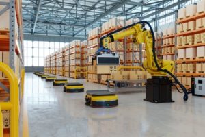
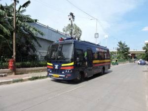
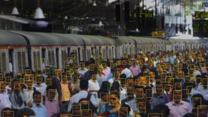
Autonomous Robots: NVIDIA Jetson is driving the new era of autonomous robotics, from security and healthcare to manufacturing, logistics, and agriculture. NVIDIA Jetson Nano, Jetson Orin, and AGX Xavier offer high-speed interface support for multiple sensors, including cameras, mmWave Radars, and IMU sensors, which enables real-time image analytics and inference at the edge. These SoMs are ideal for multi-modal autonomous robots, with advanced visual analytics that enable object detection & classification, motion planning, and pose estimation, which delivers the accuracy and fidelity to operate in factories, warehouses, and other industries. In addition, these SoMs help autonomous robots learn, adapt, and evolve using computer vision and machine learning.

When it comes to utilizing the full potential of NVIDIA Jetson SoMs for autonomous robots, there are several software options available. NVIDIA’s Isaac SDK is explicitly designed for robotics, offering a rich toolkit for developing robotic applications and making it an ideal choice for Jetson SoM users. On the other hand, NVIDIA’s JetPack SDK, tailored for Jetson SoMs, delivers comprehensive tools, libraries, and AI development frameworks. With GPU acceleration through CUDA support and deep learning model optimization using TensorRT, it stands as a robust choice for AI applications. Additionally, the widely adopted Robot Operating System (ROS) provides a flexible and modular framework for autonomous robot development. With native support for Jetson SoMs, ROS facilitates efficient sensor integration, control, and navigation capabilities, further enhancing their autonomous capabilities.

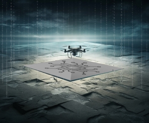
Drones & UAVs: UAVs and autonomous drones are becoming one of the most popular gadgets amongst commercial, emergency response, and military applications due to their low cost, adaptability, and capability to manoeuvre in harsh surroundings and weather conditions. UAVs use several sensors, redundancy programs to operate autonomously. The NVIDIA Jetson TX2 series is one of the fastest and most power-efficient embedded AI computing devices in the market and supports up to six cameras at 4K resolution, making it an ideal choice for battery-operated embedded systems like drones and robots. The SoM is capable of handling various functions like navigation, image processing and classification, alerts, speech recognition, data encryption and edge inference simultaneously.

In the field of Drones & UAVs powered by NVIDIA Jetson TX2, there are some great software options like PX4 Autopilot, ROS, NVIDIA Deep Learning AI, Dronekit, and AirSim. PX4 Autopilot delivers advanced flight control, while ROS offers a flexible framework which can be customized for various tasks. Deep Learning AI empowers machine learning tasks, and Dronekit facilitates custom software. AirSim provides a safe testing environment. Jetson TX2’s multi-camera support and AI capabilities make it the top choice. Together, these software options can be used to create autonomous drones that excel in navigation, image processing, speech recognition, and edge inference, ensuring safe and reliable operations.

ADAS and Driver Monitoring Systems: The automotive industry is increasingly employing advanced technologies in the quest for safer roads and minimizing accidents. A semi/fully autonomous vehicle demands an enormous amount of sensory information analysis and real-time action with no margin for error. ADAS employs many algorithms with respect to forward collision warning, road sign detection, lane analysis and lane departure warnings, etc. To perform all these complex algorithms in real-time, there is a need of powerful compute engines. The NVIDIA Jetson SoMs like Nano, TX2, Xavier NX, AGX Xavier and AGX Orin, integrated with NVIDIA TensorRT, are ideal for designing collision, lane departure and speeding warning systems. The Jetson platforms are not only the worthiest GPU-enabled platforms for autonomous systems but also power-efficient and cost-effective.

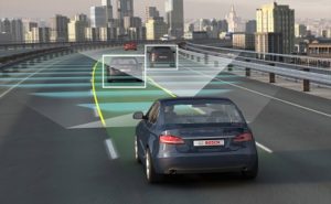
The Jetson Series can provide up to 275 TOPS performance and comes with the best in the industry machine learning and computer vision technologies. They are capable of processing immense amount of data from multiple cameras and sensors that help to give accurate driving situations in real-time. These SoMs also help in deep head pose estimation through 2D or 3D depth data through a Convolutional Neural Network (CNN), real-time traffic road signs detection by using computer vision algorithms, and real-time prediction of automotive collision risk warnings and avoidance with the help of quick visual AI systems processing.

In the world of ADAS and Driver Monitoring Systems powered by NVIDIA Jetson SoMs, software solutions play a crucial role. NVIDIA’s DriveWorks SDK, OpenCV, TensorRT, ROS, DeepStream, and NVIDIA Isaac SDK lead the pack. DriveWorks offers a comprehensive toolkit for automotive systems, while OpenCV handles computer vision tasks. TensorRT optimizes deep learning models for real-time predictions. ROS provides a modular framework, and DeepStream is ideal for analysing data. For robotics based ADAS, NVIDIA Isaac SDK offers navigation and mapping. Jetson SoMs, from Nano to AGX Orin, bring computational power and ML support to the table. Together, these software enables complex algorithms, real-time understanding of the environment, and contribute to safer roads.

Edge Camera: NVIDIA Jetson Nano, Xavier NX, and TX2 series modules are good choices for building IoT-enabled embedded vision systems and edge cameras due to their high-performance and low-power computing capabilities. These modules are ideal for processing complex data at the edge and running advanced AI workloads. The NVIDIA Jetson modules come with powerful graphics processors and AI cores that provide no limits to the implementation of versatile AI-based edge computing systems.

For Edge Cameras on NVIDIA Jetson SoMs, diverse software solutions are available. GStreamer is ideal for multimedia tasks, OpenCV offers GPU-accelerated computer vision with the help of the graphics card, NVIDIA DeepStream powers real-time analytics, Python and TensorFlow enable AI, and ROS caters to robotics. Jetson’s powerful hardware supports real-time image processing, AI analytics, and IoT. Your choice depends on the requirements, but these options deliver versatile edge computing.

Healthcare Devices: High-resolution medical imaging and its analysis are critical elements of modern healthcare. The biggest challenges to developing advanced healthcare and medical systems are high-speed low-latency data transfer, real-time analysis of the massive data and inference of actionable insights. The NVIDIA Jetson Platforms address all these concerns and help accelerate the development of next-gen medical applications that aid advanced imaging, faster diagnosis, derive the best treatment procedures and enhance surgical processes. The multiple CSI Camera support, USB 3.2, GigE (up to 10GbE), and multi-mode DisplayPort among others, facilitate high-speed data transfer between various sensors, processor, and UI for superior operational efficiency. The Jetson SoMs support H.265 and H.264 video encoding and decoding (up to 8K/30 or 4K/60), ensuring low-latency video transmission and display. These SoMs offer end-to-end software framework, datasets, and domain-optimized tools for modular and scalable AI-based healthcare product deployment.

In the world of Healthcare Devices powered by NVIDIA Jetson SoMs, a range of software options are available, all geared up to tap into their high-performance computing and real-time abilities. NVIDIA Clara, designed for healthcare, provides imaging and AI tools. MATLAB’s Medical Imaging Toolbox, with the support of Jetson’s GPU, enhances tasks related to images. TensorFlow Medical Imaging offers ready-to-use models for medical applications that use AI. PyTorch brings deep learning flexibility for custom neural networks. NVIDIA’s Deep Learning Accelerated Libraries make AI processes even faster. Jetson SoMs, with their computational abilities and imaging support, are ideal fit for healthcare devices. The software choice depends on the device’s needs, paving the path for advanced medical systems.

Vision Analytics Applications

NVIDIA Jetson powers diverse Vision Analytics applications, with a focus on Object Detection & Classification. Jetson Nano supports TensorFlow and PyTorch, making it ideal for AI vision tasks and higher versions like Xavier NX and AGX Xavier enhance tracking capabilities. Jetson TX2, Xavier NX, and AGX Xavier with Metropolis, OpenALPR, DeepStream, Pix4D, and QGroundControl, excel in real-time object detection makes them ideal for applications such as Smart Waste Management, Intelligent Traffic Management Systems, Aerial Imaging, etc.

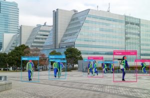
Object Detection & Classification: There is an exponential growth in object detection and classification computing due to the developments in artificial intelligence, connectivity, and sensor technologies. The NVIDIA Jetson Nano supports Machine Learning frameworks like TensorFlow, PyTorch, Caffe/Caffe2, Keras, MXNet, etc., making it an ideal platform for running AI vision tasks and AI-based computer vision applications. Jetson Nano is ideal for implementing applications such as Edge Camera, Warehouse Robots, Digital Signage, etc., demanding object detection and classification, segmentation, speech processing, image recognition, and object counting. If the application demands tracking and labelling of a detected object, developers can choose a higher version of the NVIDIA Jetson platform, like Xavier NX, Orin or AGX Xavier.

When it comes to object detection and classification on NVIDIA Jetson SoMs, two standout software options are TensorFlow and PyTorch. TensorFlow, a widely-used deep learning framework, offers robust support for these tasks. It simplifies the process with pre-trained models available through the TensorFlow Object Detection API, and it can be fine-tuned and optimized for Jetson GPUs to ensure excellent performance. On the other hand, PyTorch, another popular deep learning framework known for its flexibility and dynamic computation graph, provides pre-trained models and libraries tailored for object detection and classification. Jetson users also have the option of Jetson-specific builds, which maximize performance while harnessing PyTorch’s capabilities. These two software options provide powerful tools for addressing object detection and classification challenges on NVIDIA Jetson SoMs.

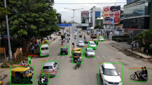
Intelligent Traffic Management: Robust, accurate, and secure traffic management systems are vital to reducing congestion and minimizing highway and city accidents. Intelligent traffic management systems help in real-time detection and classification of vehicle type, estimation of speed, queue length and vehicle flow, and traffic pattern analysis, among others. NVIDIA Jetson TX2 and Jetson Xavier NX platforms are ideal for real-time traffic management solutions because of their high computational power to fulfil specific neural network requirements, multiple 4K camera support, high-speed video encoding/decoding, real-time data communication with remote devices and the cloud network. These modules offer 10/100/1000 BASE-T Ethernet for low-latency sensor operations and power over Ethernet.

In the world of Intelligent Traffic Management, powered by NVIDIA Jetson SoMs, a versatile collection of software stands ready. NVIDIA Metropolis, an IoT platform that utilizes deep learning for real-time object prowess, while OpenALPR is ideal in license plate recognition and works fast on Jetson traffic systems because of its GPU-optimized. MATLAB is good for traffic simulation, image processing, and deep learning, especially when paired with Jetson’s powerful GPU support. NVIDIA’s TensorRT turbocharges deep learning models for traffic analysis. For controlled experimentation, DeepTraffic offers traffic simulation on Jetson SoMs. These software tools works well with Jetson’s strong computing abilities, camera support, real-time capabilities, and connectivity. All of these can help to develop intelligent traffic solutions tailored to fit specific needs.

Smart Waste Management: Waste is a surging problem for many industries. NVIDIA Jetson Modules are ideal for building smart waste management systems. The object detection and classification capability of Jetson modules helps make trash-versus-recycling decisions in an industrial environment. Equipped with high computing power, CSI Cameras and advanced image analytics powered by AI algorithms, Jetson modules can be used to build autonomous Waste Management Systems that can identify and sort infinite number of items. The AI algorithms aid the system in classifying and categorizing wastes and directing them to respective bins. Integration of digital weighing scales helps the system to easily measure, quantify and keep a detailed track of waste segregated.

In the field of Smart Waste Management, powered by NVIDIA Jetson SoMs, software options like OpenCV, TensorFlow, PyTorch, NVIDIA DeepStream, and ROS bring high-performance capabilities. OpenCV can detects and analyse waste items, TensorFlow can categorize, PyTorch can customize the waste tracking according to the needs, DeepStream accelerates waste detection, and ROS deals with waste management using robots. Jetson SoMs, with their strong computing power and support CSI Camera, are an ideal match for this task. These software tools work together to create autonomous waste management systems, boosting efficiency in identifying, categorizing, and managing waste items for improved industrial waste management.

Aerial Imaging and Surveillance: The aerial imaging and surveillance are finding several applications in domains such as Military, Survey, Forestry, Search and Rescue, Oil & Gas, Mining, Agriculture and Critical Infrastructure Protection among others. The NVIDIA Jetson Platforms are one of the finest sets of processing engines available in the market for building AI-powered Aerial Imaging solutions. High computing power, advanced graphics processing, deep-neural computing, and integration of modern AI workloads provide unparalleled image processing capabilities for these platforms. NVIDIA Jetson Tx2 and AGX Xavier are ideal for designing aerial imaging solutions that offer accelerated image processing, mapping, detection, segmentation, and tracking.

In the world of Aerial Imaging and Surveillance, where NVIDIA Jetson SoMs provide the power, there are multiple software options are available like OpenCV, TensorFlow, NVIDIA DeepStream, Pix4D, and QGroundControl. OpenCV is perfect for real-time object tracking, while TensorFlow offers tools and ready-made models for custom AI solutions. DeepStream makes it possible to process images in real-time for aerial surveillance, Pix4D can transforms images into 3D maps, and QGroundControl helps manage drone missions. All these software options work together to create efficient AI systems, which can revolutionize applications across military, agriculture, and infrastructure protection.

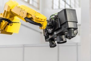
Automated Inspection: NVIDIA Jetson AGX Xavier can do miracles in the field of automated inspections and can cater to a wide range of industries and requirements. The support for multiple 4K resolution cameras, advanced machine-learning inference chores help automate inspection and identification of the smallest of defects or differences. With the help of machine-learning models, advanced AI computing, visualization, data analytics, and high-resolution simulation, Jetson AGX Xavier-powered automated inspection systems can manage routine and dangerous inspections with precision and speed.

In the world of Automated Inspection with the help of NVIDIA Jetson AGX Xavier, there is a set of great software tools available. OpenCV, with its speedier processing using GPUs, spots defects in real-time. NVIDIA’s deep learning package helps train models to detect faults. MATLAB uses advanced inspection algorithms. Cognex VisionPro is super precise for manufacturing, and MVTec Halcon is ideal for industrial inspection. These software solutions can be assembled together to create efficient AI-powered inspection systems, revolutionizing quality control across industries.

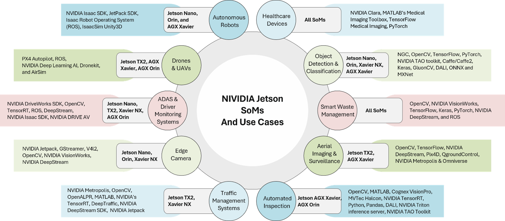
Table 1: NIVIDIA Jetson Applications

Conclusion

In a world of data-driven decision-making, the demand for AI-powered solutions will continue to grow and flourish. The NVIDIA Jetson Platforms’ flexibility, compact footprint, and high computing power offer endless possibilities to developers for building embedded systems and AI-powered devices. They offer power-efficient performance to the users to create software-defined autonomous machines.

Mistral is a Member of the NVIDIA Partner Network, and our solutions facilitate accelerated product development, prototyping and reduce time to market. Our team has unparalleled expertise and design competency in offering custom Carrier Boards, Development Platforms and Application Boards based on Jetson System on Modules. Mistral also offers feature-rich, performance-oriented off-the-shelf Carrier Boards and AI-Sensor Fusion platforms compatible with the Jetson Nano, Jetson Xavier NX and Jetson T.X2 NX and Jetson Orin NX (Available Soon) SoMs. To know more, visit mistralsolutions.com/neuron.

Aerospace and Defense Industry – Technology Trends in 2024

The Indian Aerospace and Defense Industry is a critical sector for India’s economy and national security. The Indian A&D sector has made significant strides in recent years, with India becoming one of the largest importers of defense equipment. However, the government has been pushing for greater indigenization of defense equipment and the industry has responded positively with increased focus on research and development, emphasis on developing advanced systems and technologies, collaboration with international partners, push towards receiving technology knowledge, and increased investment in defense sector. Programs like Indian Defense Offset and Make in India are also promoting increased global participation in the Indian Aerospace and Defense segment.

Leading Aerospace and Defense OEMs are constantly striving to adopt modern technologies to remain competitive and enhance their product capabilities. From Additive Manufacturing, Artificial Intelligence & ML, to Augmented Reality and Digital Twins, OEMs are adopting many game-changing technologies in the aerospace and defense industry.

Let’s look at some of the trending technologies that are expected to augment the Indian Aerospace and Defense segment in the near future.


Stealth

Stealth technology is a combination of techniques that diminish the emission and reflection of visible light-heat signatures, sound, and radio signals by the vehicle surface. While no aircraft is completely invisible to RADARs, stealth aircraft make it more challenging for conventional RADARs to detect and track them. Stealth technology in aerospace and defense encompasses several key aspects which includes use of multiple substrates and techniques. Visual Stealth involves camouflage the aircraft to blend with their surroundings, often using dark colors for nighttime operations. Infrared Stealth focuses on reducing the infrared (IR) signature caused by heated surfaces, achieved through engine placement, air mixing, shielding, and coatings. Acoustic Stealth aims for minimal noise emissions to evade acoustic detection. Achieving this involves engine and airframe design, exhaust systems, and active noise reduction. Radar Stealth is achieved by absorbing or deflecting radar waves using specially coated materials.

Several countries around the world are actively investing in and advancing stealth technologyAerospace and Defense within the aerospace and defense sector. These efforts are aimed at enhancing the stealth characteristics of various military platforms, including aircraft, naval vessels, and ground vehicles. These advancements include the design of stealth airframes, radar-absorbing materials, and innovative sensor systems to reduce the detectability of vehicles and improve their survivability in modern combat scenarios. Additionally, research and development in stealth technology continue to be a focus, with ongoing efforts to refine and evolve these capabilities to maintain a competitive edge in the evolving landscape of aerospace and defense capabilities.

India’s plan to manufacture a stealth aircraft is going to turn into reality as the Advanced Medium Combat Aircraft (AMCA), fifth-generation stealth, multirole combat aircraft program has progressed to Critical Design Review phase. The AMCA is being developed by the DRDO and HAL and is expected to feature advanced stealth technologies such as RADAR-absorbing materials, advanced avionics, and reduced RADAR cross-sections. The Indian defense industry is also focusing on developing stealth unmanned aerial vehicles (UAVs), which can be used for surveillance and reconnaissance missions.

Artificial Intelligence and Machine Learning

The Indian Aerospace and Defense industry is taking massive steps in transforming the defense forces. The industry is embracing modern technologies to add intelligence to defense forces and deployments. Bold policies and the drive towards indigenization have created an atmosphere for groundbreaking innovation and collaboration. The collaborative effort by research institutes, academic institutions, public and private industry, and start-ups has helped create many unique AI & ML based technological products in areas such as surveillance, data, and logistics.

The use of AI & ML aids developers/users to gather crucial information and performance data of various components in a mission-critical platform. This will help them continually enhance product performance, minimize errors, monitor the health of electronics within aircraft, and manage safety concerns effectively. AI and Machine Learning enable Autonomy in ISR (Intelligence, Surveillance, and Reconnaissance), and data management, which will benefit in combating terrorism, implementing counter-terrorism measures, and safeguarding assets.

The use of advanced AI analytics, computer vision systems and geospatial data processing can help identify, locate, and categorize imminent threats. AI-powered military robots, unmanned vehicles like battle tanks and aircrafts can make decisions faster and act swiftly in battlefield.

Indian Aerospace and Defense organizations are making significant strides in harnessing Artificial Intelligence (AI) and Machine Learning (ML). Some of the projects includes underwater threat detection using AI & ML, development of AI-driven multi-role, advanced and long-endurance drones to step up vigilance strategically in high-altitude Northern and North-eastern border areas, and using AI & ML for surveillance and reconnaissance operations. These initiatives underscore India’s commitment to enhancing defense capabilities through AI and ML.

Robotics and Unmanned Systems

Aerospace and DefenseRobotics and Unmanned Systems are rapidly advancing and becoming increasingly popular in
the Aerospace and Defense industry. These systems are programmed to perform tasks independently as well as under human supervision. Robotics and Unmanned Systems can be equipped with various sensors and tools. Some examples of unmanned systems include drones, unmanned ground vehicles (UGVs), and unmanned underwater vehicles (UUVs).

Robotics and Unmanned Systems are getting popular in the Aerospace and Defense industry as they help to cut the operational cost and increase efficiency. Cost and risks associated with human workforce in an operation in a hazardous environment can be overcome by using robots and unmanned systems. These systems can operate and perform high-risk tasks for extended hours with increased efficiency and productivity, thereby reducing or eliminating the risk of injury or loss of life for human operators.

Indian Aerospace and Defense organizations have undertaken numerous prominent projects inAerospace and Defense the realm of Robotics and Unmanned Systems. One initiative focuses on an electrically powered, fully automated, remotely operated vehicle for tasks like bomb disposal and handling hazardous materials. Another project involves a versatile unmanned ground vehicle capable of autonomous navigation using GPS waypoints and equipped with obstacle detection and avoidance capabilities for military applications, including mine clearing, surveillance, and operation in contaminated zones. Additionally, there is an effort dedicated to developing indigenous Unmanned Aerial Vehicles (UAVs) for surveillance and reconnaissance. Another initiative involves a versatile multi-mission UAV, capable of battlefield surveillance, reconnaissance, target tracking, localization, and artillery fire correction, launched from a mobile hydro-pneumatic launcher with day/night capabilities. These initiatives reflect India’s commitment to enhancing its defense capabilities through the integration of Robotics and Unmanned Systems, with a focus on improving operational efficiency and safety while maintaining a strategic advantage.

A long way to Go!

The advancements in technologies such as Stealth, Counter-surveillance, Artificial intelligence, Machine Learning, Cybersecurity, Robotics, and unmanned systems are transforming the Aerospace and Defense industry. These technologies will bring numerous benefits to the Aerospace and Defense sector, enabling increased efficiency and productivity while minimizing risks to military personnel. Upgrades and technology updates are expected to continue to enhance the industry further. As such, the Aerospace and Defense industry in India is poised for growth and development, as technology continues to play a critical role in ensuring the safety and security of the nation.

NVIDIA Jetson SoMs – Capabilities and Use Cases – Part: 1

Autonomous machines, robotics and artificial intelligence have been transforming daily life, Nvidia Jetson Nano, NVIDIA Jetson TX2 NX, NVIDIA Jetson Xavier NX , nvidia jetson nano developer kitmaking it more convenient, safe and efficient. These technologies are being applied to multiple applications in domains such as industrial, automotive, healthcare, smart city, smart buildings, and entertainment among others. The ever-evolving technology landscape and the increasing need for real-time data processing and inference at the edge is encouraging SoC/GPU manufacturers to build powerful edge computing devices that can run modern Deep Learning (DL) workloads. NVIDIA Jetson System on Modules (SoMs) – namely NVIDIA Jetson Nano, NVIDIA Jetson TX2 NX and NVIDIA Jetson Xavier NX are embedded AI computing platforms designed to accelerate edge AI product lifecycle. These high-performance, low-power compute engines are built to run complex computer vision, robotics, and other low-power applications. In addition, NVIDIA offers CUDA-X libraries, a set of highly optimized, GPU-accelerated libraries. CUDA-X offers a robust programming environment that works seamlessly with all Jetson SoMs, enabling customers to seamlessly use their application across various Jetson Platforms.

Advantages of NVIDIA Jetson Platform

Versatile Hardware – The NVIDIA Jetson portfolio provides a wide range of high-performance, low-power system on modules, that feature multi-core ARM cores, NVIDIA GPU, AI computational performance up to 275 TOPS and a host of high-speed interfaces, ideal for complex DL pipelines.

Unified Software offers Ease of Development – NVIDIA Jetson System on modules and Development Kits are supported by a unified software architecture that helps developers to expand or enhance their product portfolio on different Jetson modules without further coding. This unified approach helps enterprises to create product portfolios with a significant return on investment.

Cloud Native Support for Scalable Deployments – Cloud-native technologies and workflows like orchestration and containerization are supported by all NVIDIA Jetson platforms, which accelerate edge AI product development, agile deployment, and management throughout the product lifecycle. Frequent updates and constant upkeeps are imperative to rapidly improve AI efficiency.

Here’s a sneak peek of the hardware capabilities of various Jetson Modules:

The Jetson AGX Orin is the latest incorporation from NVIDIA Nvidia Jetson Nano, NVIDIA Jetson TX2 NX, NVIDIA Jetson Xavier NX , nvidia jetson nano developer kitamong all Jetson Modules. This SoM is one of the most powerful embedded processors currently in market, with up to 275 TOPs performance. The Jetson AGX Orin offers a giant leap forward in Edge AI and robotics. Jetson AGX Orin offers 8x performance over Jetson AGX Xavier with configurable power between 15W and 50W, making it ideal for autonomous machines and advanced robots. It will also help developers to deploy complex and large AI models to solve problems such as 3D perception, natural language understanding, and multi sensor fusion. This SoM supports multiple concurrent AI inference pipelines with onboard 64GB eMMC, 204 GB/s of memory bandwidth, and high-speed interface support for multiple sensors.

The NVIDIA Jetson Orin NX provides high-speed interface support for multiple sensors, offers twice the CUDA cores, 5x performance of NVIDIA Jetson Xavier NX and 3X the performance of Jetson AGX Xavier for power-efficient autonomous machines. This module offers up to 100 TOPS of AI performance, 1024-core NVIDIA Ampere architecture GPU with 32 Tensor Cores, power configurable between 10W and 25W, supports external NVMe, shares the form factor compatibility with NVIDIA Jetson Xavier NX, and can give a tremendous performance in an amazingly compact package.

With the launch of the new Jetson Orin Nano SoM, NVIDIA Jetson is setting a new standard for entry-level edge AI and robotics. Orin Nano comes in two variants, and it can deliver up to 80x the performance over the previous generation, up to 40 TOPS of AI performance, and comes with 5W and up to 15W power options. Jetson Orin Nano includes a video decode engine, 6-core Arm Cortex-A78AE CPU, ISP, audio processing engine, video image compositor, and video input block. This new SoM series also features up to 1024-core NVIDIA Ampere architecture GPU with 32 Tensor cores, supports FP16 and Int 8, and comes with 4GB and 8GB. This SoM comes with a strong Ecosystem, better software support, enhanced encoding capabilities, and memory bandwidth and supports external NVME for data storage directly as it has no eMMC.

Nvidia Jetson Nano, NVIDIA Jetson TX2 NX, NVIDIA Jetson Xavier NX , nvidia jetson nano developer kitThe NVIDIA Jetson AGX Xavier is a power-efficient module designed for autonomous machines
that delivers up to 32 TOPS of AI performance. This compact module includes high-speed I/O and hardware acceleration for the entire AI pipeline enabling developers to come up with the latest AI applications. The Jetson AGX Xavier also provides an extended temperature range, vibration and shock specifications, making it one of the best choices for safety-certified and industrial-grade products. This SoM comes with NVIDIA Volta architecture GPU with 512 CUDA cores, 8-core NVIDIA Carmel Armv8.2 64-bit CPU and support up to 6 CSI cameras in addition to the host of the display, connectivity and networking interfaces.

The NVIDIA Jetson Xavier NX is a small form-factor module, in the size of a credit card that offers up to 21 TOPs of accelerated AI computing. This module can process data from various high-resolution sensors and run multiple advanced neural networks in parallel, which is critical to modern embedded systems. The 384-core NVIDIA Volta™ GPU with 48 Tensor Cores offers high computing power for compact, intelligent machines like autonomous drones and portable medical devices. The module comes with 6-core NVIDIA Carmel ARMv8.2 CPU, dual DLA engines, 8 GB memory, 6 CSI camera and support a host of display, connectivity, and networking interfaces.

The NVIDIA Jetson TX2 NX is a power-efficient (7.5W) embedded AI computing device that offers up to 2.5x the performance of Jetson Nano. The module features a variety of standard hardware interfaces that makes it ideal for designing a wide range of small form-factor products that run advanced machine learning applications. The Jetson TX2 modules integrate NVIDIA Pascal™ GPU architecture with 256 NVIDIA CUDA cores, dual-Core NVIDIA Denver 2 64-Bit CPU, 8GB 128-bit LPDDR4 memory, and 32GB eMMC 5.1 storage. In addition, TX2 offers USB 3.0 Type A, USB 2.0 Micro USB (supports recovery and host mode), HDMI, M.2 Key E, PCI-E x4, Gigabit Ethernet, full-size SD, SATA Data and Power, GPIOs, I2C, I2S, SPI, CAN, TTL UART with flow control, display expansion header, and camera expansion header.

The NVIDIA Jetson Nano is a small, power-efficient, Nvidia Jetson Nano, NVIDIA Jetson TX2 NX, NVIDIA Jetson Xavier NX , nvidia jetson nano developer kit high-performance AI computing device to run AI applications, process data from high-resolution sensors and run multiple neural networks in parallel. This module is an ideal entry-level option to add advanced capabilities to embedded products and elementary solutions like intelligent gateways or entry-level NVRs. The Jetson Nano has an integrated 128-core Maxwell GPU, quad-core ARM A57 64-bit CPU, 4GB LPDDR4 memory, and support for MIPI CSI-2 and PCIe Gen2 high-speed I/O.

Nvidia Jetson Nano, NVIDIA Jetson TX2 NX, NVIDIA Jetson Xavier NX , nvidia jetson nano developer kit

NVIDIA Jetson Modules _ Spec Comparison

Conclusion

The NVIDIA Jetson System on Modules are power-performance-optimized edge devices that can
transform every industry, including healthcare, retail, manufacturing, transportation, construction, logistics, agriculture, robotics, surveillance, and more. AI-based embedded product companies and developers are using NVIDIA Jetson SoMs to enhance and accelerate product development, demonstrating how cutting-edge technologies can facilitate new levels of success every day. Mistral is a Member of the NVIDIA Partner Network, and our solutions facilitate accelerated product development, prototyping and reduce time to market. Our team has unparalleled expertise and design competency in offering custom Carrier Boards, NVIDIA jetson nano developer kit and Development Platforms and Application Boards based on Jetson System on Modules.

Mistral also offers feature-rich, performance-oriented off-the-shelf nvidia jetson nano developer kit, Carrier Boards and AI-Sensor Fusion platforms compatible with the Jetson Nano, Jetson Xavier NX and Jetson TX2 NX SoMs. To know more, visit mistralsolutions.com/neuron. Stay tuned for the second part of the blog that features various use cases of Jetson platforms!

High-performance, Real-time 4K / HD Video Streaming Designs

Real-time surveillance and remote monitoring are gaining large importance in a wide range of industries such as Oil and Gas, Power Grid, Industrial Automation, Smart Buildings, etc. The demand for high-quality real-time HD Video Streaming / 4K Video Streaming designs in surveillance applications is higher than ever and this calls for compute-intensive image processing designs and advanced encoding and decoding techniques. Advanced camera architectures include an onboard microprocessor or FPGA with visual analytics and image processing algorithms for pixel pre-processing and decision-making within the camera. Complemented by AI Algorithms, these advanced cameras facilitate real-time communication with the central command center and stream footages of significance to aid user-level decision making. 4K Video Streaming Camera, Digital Video Designs, HD Video Streaming , 4K Video Streaming, HD Video StreamingThe advent of digital technologies and rapid development in Sensor technologies and embedded electronics, particularly the arrival of compute-intensive SOCs, high-speed DSPs, high-speed wireless / wired interfaces, video streaming protocols and cloud technologies among others enabled cameras to go beyond traditional surveillance and facilitate advanced AI-based vision applications such as safe-zone monitoring, No-go zone, object detection, etc. The design and implementation of a high-speed, real-time 4K video streaming camera requires expertise in a wide array of embedded technologies. This article is an attempt to dive a little deeper into the design of a high-end real-time HD video streaming designs / 4K video streaming designs for camera in surveillance applications. We explore the basics of camera architecture and video streaming along with several streaming protocols, selection of sensors and processing engines, system software requirements and cloud integration among others.

4K Video Streaming – Camera Design Considerations

– Key System Components

Image Sensors

4K Video Streaming Camera, Digital Video Designs, HD Video Streaming , 4K Video Streaming, HD Video StreamingThe image sensor is the eye of a camera system which contains millions of discrete photodetector sites called pixels. The fundamental role of sensors is to convert light falling on the lens into electrical signals, which in turn will be converted to digital signals by the processor of the camera. Image sensors make a big impact when it comes to the performance of the camera due to various factors such as size, weight, power and cost. Choosing the right sensor is key to the design of a high-quality camera for surveillance applications. Selection of the sensor is influenced by several factors such as frame rates, resolution, pixel size, power consumption, quantum efficiency and FoV among others.

Sensor Interface

The selection of sensor interface is another critical factor that impacts the performance of a real-time 4K video streaming camera. The MIPI CSI (1/2/3) is one of the most preferred sensor interfaces currently in use. Since MIPI CSI offers a lean integration, several leading Chip manufacturers such as NXP, Qualcomm and Intel among others are adopting this technology for industrial and surveillance markets. CMOS sensors with MIPI CSI interfaces enable quick data transfer from the sensor to the host SoC of the system, facilitating high-speed and system performance. Developers can also use high-speed interfaces such as GMSL and FPD Link in applications where the processing of signals happens at a different platform or system. These interfaces greatly impact the overall performance of the camera, which is key to real-time 4k video streaming applications.

4K Video Streaming Camera, Digital Video Designs, HD Video Streaming , 4K Video Streaming, HD Video Streaming

Key Components of a 4K Video Streaming Camera

Camera Interfaces

Identifying the right camera interface with high-speed video streaming feature is equally critical. A developer can rely on high-speed interfaces such as USB 3.2, CoaXPress 2.0, Thunderbolt3, DCAM, CameraLink HS (Framegrabber) and Gigabit Ethernet, among others.

Signal Processing Engines

There are numerous SOMs and SBCs based on leading GPUs, SOCs and FPGAs in the market, which are ideal for a high-end video streaming camera design. Identifying the right processor from this large pool might be a tough task. The processing engine must support the ever-evolving video encoding, decoding and application processing requirements of the camera system. In addition, the processor should aid key camera parameter settings like autofocus, auto exposure, and white balance along with noise reduction, pixel correction and colour interpolation, among others. The advent of hardware accelerated video encoding (GPU) and 4K Video streaming is greatly enabling imaging applications, especially surveillance and machine vision applications by providing breakthrough performance.

GPUs offer more computing power over a CPU, which is indispensable to high-performance, real-time 4K video streaming designs. Processing platforms that support hardware accelerated media encoding and decoding would be an ideal choice for camera developers. Cameras meant for HD / 4K video streaming applications must be of high resolution, high frame rate, industry-leading image compression and streaming capabilities, and low power consumption. Advanced low-power embedded processors with built-in video analytics are gaining high popularity among developers as they aid real-time video streaming and communication. HD video streaming cameras with edge computing capabilities are ideal for time-sensitive applications and help make intelligent decisions at the edge. Such systems are highly recommended for remote applications, where there is limited no connectivity to cloud or a central command center.

– System Software

Operating System

4K Video Streaming Camera, Digital Video Designs, HD Video Streaming , 4K Video Streaming, HD Video Streaming

4K Video Streaming – Software Architecture

Despite the emergence of several operating systems, Linux rules the embedded world. Linux is ideal for HD Streaming Camera designs due to its stability and networking capabilities. As Linux is an open-source operating system, developers can easily and quickly make changes and redistribute it. One can meet the unique requirements of the project using Linux, while easily addressing critical factors including power consumption, data streaming, and any other challenges imposed by the hardware configuration or other software elements. Linux also allows easy customization and integration of I/Os and enables faster time to market.

Sensor Drivers

Sensor driver development and integration is another crucial part of camera design. Most of the sensor modules come with drivers, however developers can also write camera sensor driver as per the specific needs of the end product. Sensor drivers should address several key components such as clock frequencies, frame size, frame interval, signal transmission, stream controls, sensor power management and sensor control framework among others. In addition, developers have to address sensor interface design, protocol development and integration as well.

OpenCV

OpenCV, computer vision library has become the most popular image processing platform among the developers of imaging solutions in recent years. Developers can use OpenCV libraries to implement advanced image processing algorithms in their video streaming solutions. The platform offers more than 2000 algorithms related to image processing. Since OpenCV libraries are written in C++, developers can easily integrate these software stacks into their designs. OpenCV enables the developers to focus on video capture, image processing and analysis including features like face detection and object detection. OpenCV also offers storing, reading and writing images in an n-dimensional array and performs image processing techniques such as image conversion, blur, filtering, thresholding, rotation, scaling, histogram equalization, and many more.

Algorithms

4K Video Streaming Camera, Digital Video Designs, HD Video Streaming , 4K Video Streaming, HD Video StreamingAlgorithms can be implemented at two layers in a high performance, real-time video streaming camera design. While the first layer specifically caters to image processing, the second layer of algorithms adds intelligence to the visuals captured. High-definition cameras capture images in high detail. However, the data captured may need further enhancements for effective analysis and accurate decision making. Implementation of visual algorithms, especially those aid in image correction and enhancement has become a minimal requirement for modern surveillance cameras. The commonly implemented algorithms include autofocus, auto exposure, histogram, color balancing, and focus bracketing among others. The second layer of algorithm is implemented on advanced surveillance cameras that leverage complex visual analytics powered by AI-algorithms to provide real-time situational awareness. These systems combine video capturing, processing, video analytics and real-time communication for effective situational awareness and decision making. These 4K Video Streaming cameras are finding increased applications in automated detection of fire, smoke, people counting, safe-zone monitoring, facial recognition, human pose estimation, scene recognition, etc.

Key Performance and Feature Considerations

HD / 4K Video Streaming

High-definition video streaming (4K Video Streaming) is getting more popular, however, in industrial and surveillance applications, real-time HD video streaming poses many challenges due to the enormous amount of data the system handles. The transmission of large volume of data to a remote system with minimal latency is a major challenge in HD / 4K video streaming. This can be addressed to a great extent by selecting appropriate processors, preferably FPGAs. FPGA has several benefits over conventional processors and the developers can easily integrate complex video analytics algorithms in the device. The availability of a large number of logic cells and embedded DSP blocks and flexible connectivity options make FPGA a powerhouse that can handle faster image processing and real-time 4K video streaming.

Video Compression

Raw video files are digitized, compressed and packetized by the processor for faster transmission to the remote monitoring system. Cameras use various video compression technologies and algorithms to compress a video, which can be further reconstructed by the host PC to its original resolution and format. Developer can use standards such as MJPEG, MPEG-4, H.263, H.264, H.265, and H.265+ for image compression for easy transfer.

Video Streaming Protocols

4K Video Streaming Camera, Digital Video Designs, HD Video Streaming , 4K Video Streaming, HD Video Streaming

4K Video Streaming – Protocols

For real-time video streaming over a network, several video streaming protocols can be implemented in cameras. The commonly used protocols include Real-Time Streaming Protocol (RTSP), which acts as a control protocol between streaming severs (camera and the host PC) and facilitates efficient delivery of streamed multimedia, Real-time Transport Protocol (RTP), transports media stream over the network and HTTP, a protocol that provides a set of rules for transferring multimedia files including images, sound and video over IP networks. The RTSP in conjunction with RTP and RTCP, supports low-latency streaming, making it an ideal choice for high-speed streaming Camera designs.

Small Form-factor, Low-power Design

Today, embedded product developers are competing to reduce the size of their products while increasing the efficiency manifold. The advent of low power, small form-factor multi-core SoCs, graphic accelerators and memory technologies is aiding designers to build small footprint, power-efficient cameras. Industrial and surveillance cameras demand low-power designs due to the nature of their deployment. Such cameras designed for demanding environments must offer low energy dissipation while maximizing battery life. Developers can also consider PoE for wired camera designs. Surveillance systems heavily rely on either NVRs or cloud storage to save video footage for future references and analysis. Since a physical network connectivity is important for wired applications, PoE ensures that the camera is always powered and connected.

4K Video Streaming Designs require multiple disciplines

Real-time HD video streaming is a need of the hour. From Industrial robots to sophisticated drones, security and surveillance to medical applications, high-quality imaging is finding a crucial role in embedded world. Advanced cameras are capable of capturing and transferring a large amount of data, leveraging high-speed industrial interfaces and protocols. The idea of this Blog is to understand the fundamental components and explore key design considerations while developing a high performance, real-time video streaming camera for surveillance applications.

By using leading SOCs, latest sensors and integrating various image processing and streaming platforms, one can develop a state-of-the-art camera for real-time video streaming. Mechanical design including Sensor housing, meeting environmental and temperature standards are also critical to the successful design of a camera. As a developer one should have expertise in selection and integration of camera sensors, HD video streaming protocols, implementation of system software and sensor drivers, development and integration of camera interfaces, image signal processing, sensor tuning, image/video compression algorithms, image enhancement techniques, etc. to realize a high-end real-time video streaming design.

This blog is a concise version of the Article ‘Real-time HD video streaming for surveillance applications’ by Mistral Solutions, published in Electronic Specifier.


Automotive Antenna Technologies for Automotive Applications

The global automotive market is expected to grow at a CAGR of 4.5% over this decade according to Market Research Future. The key drivers for the growth are increasing demand for connected vehicles, autonomous vehicles, advanced infotainment systems, ADAS, and emergence of smart Traffic and Road safety applications. As we strive to achieve full autonomy of vehicles, which is fast becoming a reality, we will witness higher number of sensors getting employed in vehicles as well as intelligent, connected external transport infrastructure. One of the essential components of automotive systems – be it in-vehicle, or with infrastructure outside vehicle – that enable wireless communication is RF Antenna. Antenna technologies are also greatly enabling related technologies like network connectivity, Global Navigation Satellite System (GNSS), Global Positioning Systems (GPS), Vehicle-to-everything (V2X) leveraging the higher speed and security of 3G, 4G, LTE, and more. Automotive antenna usually operate in frequencies ranging from AM band (535-1605 kHz) to the millimetre-wave band (24GHz, 77 – 81GHz).

Automotive Antenna Systems

Today’s vehicles are loaded with a number of advanced Electronic Systems. These systems aid safe and secure driving, offer seamless connectivity and provide numerous entertainment choices to driver and passengers.

  • In-vehicle Infotainment Systems – Advanced in-vehicle infotainment systems integrate Digital Audio Broadcast (DAB), Satellite Radio, Smartphone connectivity, Navigation, gaming systems, Instruments Cluster, ADAS Display, Heads-up Displays, Telematics, etc. into one ecosystem called integrated cockpit
  • V2X Communication – Systems that enable communication between vehicles or with road safety infrastructure, pedestrians or WAN
  • Advanced Driver Assistance System (ADAS) – Enables a safe and secure driving experience by providing alerts on Object Detection, Lane departure, Pedestrian Detection, Traffic Signal Recognition, in addition to Adaptive Cruise Control, Park Assist, Collision Avoidance, Blind Spot Detection, Automatic Emergency Breaking, Driver Monitoring among others. ADAS accurately evaluate risk and adapt driving appropriately to each situation without or minimal involvement of human

Automotive Antenna Design, Automotive V2X Communications, Automotive Antenna

These systems are enabled by various types of Automotive antenna and sensors operating at different frequencies, offering detection, identification, classification and wireless data communication. In this blog, we look at a few commonly used Automotive antennas,  technologies and their applications.

Types of Automotive Antenna

The automotive antenna ecosystem can be broadly classified into two categories – Planar and Non-planar Antennas. While Planar Antennas are increasingly used in in-vehicle communication and ADAS applications, Non-planar Antennas are primarily used for V2X communications.

Planar Antennas

Planar Antennas are becoming popular in Automotive sensing applications due to their low cost, low profile (more compact and lightweight) and ease of integration on host platforms. These antennas meet the fundamental requirements of various automotive applications due to high gain, and low loss. The low profile of these antennas also facilitates easy integration without hampering the aesthetic signature of vehicles. One of the key advantages of planar antennas is the convenience they bring in to form large array structures combining various elements such as microstrips and patches, providing narrower beams and better angular resolutions. Designers prefer Planar Antennas to form phased and conformal arrays and can support linear and circular polarization based on the design used. Planar antennas are commonly used for wireless communication systems such as FM, AM, TV, Wi-Fi, and DAB audio reception, in automotive vehicles and are installed under an aperture in the roof of a vehicle.

Microstrip Patch Antenna

Microstrip Patch Antennas have become very popular in recent decades due to their thin planar profile which can be incorporated onto the surfaces of consumer products, cars, aircraft, and missiles. These planar antennas have low profile, low cost, and are conformable to planar and non-planar surfaces. They can be easily fabricated and integrated to communication systems as they are printed on circuit boards directly. The printed circuit technology also provides high dimensional accuracy, which is usually tough to achieve using conventional antenna fabrication methods.

A typical Microstrip Antenna has a radiating patch on one side and a ground plane on the other side.Automotive Antenna Design, Automotive Planar Antenna, Automotive Antenna, Microstrip Patch Antenna Microstrip patch antennas can be of various shapes (rectangular, circular, ring, triangle, quintuple, etc), designed to match specific characteristics of the application. They are commonly used in SDARS satellite communication, WLAN and Car-2-Car Communication, GPS systems. These antennas are unobtrusively flat and can be easily employed in a vehicle’s structure, typically behind a fender or bumper.

Stacked Patch Antenna

Microstrip Patch Antennas, despite being gaining a lot of popularity, have their own restrictions as well, especially the narrow bandwidth in terms of impedance, circular polarization axial ratio, gain level, etc. Achieving higher efficiency for antennas have always been a challenge and a top priority for designers. And, one of the recently adopted methods to overcome the limitations of Microstrip Patch Antennas is stacking of multiple patches, which is known as stacked patch antenna. In a stacked patch antenna, two substrates are being used to improve the antenna performance. The method of stacking patches is realized through electromagnetic coupling. The method offers enhanced operating bandwidth, lower cross polarization, better antenna gain, directivity and increased efficiency. Stacked Patch Antennas are increasingly employed in vehicles for faster and efficient Satellite Communications, Wireless signal-tracking, SDR, WLAN, etc.

UWB Patch Antenna

Another Planar Antenna which is harnessing lot of popularity among Automotive Wireless System designers. Microstrip Patch Antennas have a typical frequency bandwidth of 7% which may not meet the needs of modern wireless technologies. This limitation can be overcome by using Planar UWB antennas, which has wider bandwidth and monopole like pattern. Due to wider bandwidth, higher data rate, low power consumption, less complexity and relatively low cost of fabrication, UWB Patch Antennas becoming a key component in automotive environment and other wireless communication applications. UWB Antennas operates in the frequency range of 3.1–10.6 GHz and are designed to exhibit omnidirectional radiation characteristics. These antennas are ideal for short-range communication, to transfer data over wide frequency bands above 500MHz. UWB antennas enable remote car management by pairing with user’s phone to lock and unlock doors, enhanced security, improved V2X engagement, etc.

Chip Antenna

Automotive Antenna Design, Automotive Planar Antenna, Automotive Antenna, Automotive Chip AntennaChip Antennas are compact, low-profile and offers high performance and reliability. They are designed for easy integration into wireless communication systems. In an automotive environment, Chip Antennas of various bandwidth is employed to establish in-vehicle and vehicle-to-infrastructure connectivity. Antennas for BLUETOOTH, WLAN, Cellular, GNSS, DSRC, SDARs, etc. are now coming in Chip, making it more compact and efficient.

Patch Antenna Array for 24GHz / 77GHz SRR and LRR

Antenna arrays are a combination of multiple identical antennas that help generate more powerful radiation of particular shape. The gain and directivity are relatively higher in antenna arrays compared to the single element antennas. Antenna arrays are considered the best method to design low-profile, high-performance antennas due to their high gain and directivity, low mutual coupling between the array elements and low side/rear lobes. The geometry and the position of antenna elements, the distance between the elements, excitation phases, and the radiation pattern of each element defines the beam formation.Automotive Antenna Design, Automotive Planar Antenna, Automotive Antenna, 77GHz Patch Antenna Array

The 24GHz and 77GHz low-profile printed antennas are becoming the most essential components ADAS and Autonomous applications due to their multifunctional capabilities and high precision. Three types of radars are used in ADAS and Autonomous platforms for object detection and collision avoidance – Short-range Radar (0.5-20m), Medium-range Radar (1-20m) and Long-range Radar (10 – 250m).

The 24GHz and 77GHz mmWave Radars can be designed based on various antenna patterns. Some of the popular antenna types used for SRR and MRR Applications are Microstrip Patch Antenna Array, Microstrip Grid Antenna Array, Microstrip Comb Antenna Array, Circular Grid Antenna Array, Planar Dual-Polarized Microstrip Patch Antenna, etc. We have already discussed that; planar elements can form array structures by merging simple microstrip patches. This is the basic principle behind designing 77GHz mmWave antennas. The grid arrays provide improved beam scanning with a wide bandwidth of 4 GHz in the frequency range of 77–81 GHz. Number of transmitting and receiving elements (typically microstrip patches) can vary based on the end application.

Non-planar Antennas

Non-planar Antennas are typically Patch Antennas integrated on a curved or non-planar surface (substrate). Typically, these antennas are fabricated using flex substrates which can be molded on to a nonplanar surface. Non-planar Antennas are relatively complex compared to Planar Antennas, due to its geometry and fabrication challenges. The designers have to consider the impact of flexing the substrate on the impedance of the antenna. The common planar antennas used in Automobiles are Monopole Antenna (Also known as Whip Antenna) and Sharkfin Antenna.

Monopole Antennas (Whip Antenna)

This is one of the most popular antennas that enables a broad range of applications, from VHF sound broadcasting to car-2-car communication. A Monopole Whip Antenna consists of a foot and a rod and is usually placed on the centre of the roof of a car. Alternatively, they can be placed on an edge of the roof or on bumper. Whip antennas are ideal for VHF, UHF, Cellular, LTE, and WLAN applications in Automobiles. Due to competitive pricing and easy integration on vehicles, Whip antennas are among the most preferred in automotive industry.Automotive Antenna Design, Automotive Non-planar Antenna, Automotive Antenna, Automotive Whip Antenna

Monopole Whip Antennas, however, bring two major drawbacks. These antennas are significantly large and protrude over the vehicle roof, impacting aesthetic signature of the vehicle. Thus, Automotive OEMS are now keen on adopting newer technologies and designs that assure higher efficiency, but has least impact on the visual coefficient of the vehicle. Another drawback of monopole whip antennas is their narrow bandwidth, which limits its capability to transmit receive signals of varying frequencies. The research to overcome these drawbacks eventually resulted in the innovation of Sharkfin Antennas.

Sharkfin Antenna

Sharkfin Antennas are more recent innovations compared to other conventional antennas employed in an automotive ecosystem. These antennas are gaining popularity as they are more functional, aesthetically appealing and rugged. Sharkfin Antennas are more compact in size and consists of multiple antenna elements catering to multiple applications. For example, a sharkfin antenna can include multiple of PIFA (supports MIMO-LTE), V2V antennas working at 5.9 GHz, WiFi (can support dual bands at 2.4 GHz and 5 GHz), patch antenna for GPS application, etc.

The co-existence of multiple antennas catering to multiple application within the compact shark-fin case is a design challenge, as it can impact the efficiency due to the mutual coupling effect. However, a perfectly designed Sharkfin antenna offers high gain and superior performance for applications such as navigation, tracking, communication, SDAR, V2V communication, WiFi, etc.

Antenna Placement

With the emerging trend of self-driven vehicles, a large number of antennas and sensors are getting employed on vehicles. The key question is, where to place these antennas?

For any antenna, proper placement is fundamental to optimal performance. Antennas should be decoupled from any other conducting parts and sensors of the vehicles. If they are not used in the right way, the efficiency will be compromised to a great extent.

Automotive Antenna Design, Automotive Antenna Positioning, Automotive Antenna

The roof of the car is considered as the ideal place for integrating antennas, as it fulfils fundamental requirements – high above the ground and least obstructed – providing good spatial coverage along the horizontal plane. Omnidirectional (AM/FM, GSM, 3G, LTE, WiFi, V2V) and directional antennas (Navigation, SDARs, Satellite Radio, 24/77GHz) can ideally go into roof of the vehicle. Shark-fin antennas (which are typically a combination of antennas catering multiple services), rod antenna and satellite antennas are typically placed on roof.

Mounting multiple antennas into rear spoilers and concealing them under polymer composite panel on roof are developments pioneered by Toyota and Volvo in 1990s and early 2000s. By embedding multiple antennas into the spoiler and roof, designers could efficiently optimize the use of the space without compromising the aesthetic appeal. Telephoning and satellite broadcasting SDARS antennas, Sound and TV broadcasting VHF-antennas, GPS-antennas, and Car-2-Car Communication antennas are some of the antennas that can be integrated into the spoiler.

In the absence of rear spoilers, antennas can also be placed into the rear windscreen. As an alternative, side windows are also preferred, however, the smaller size of the window may bring in challenges while accommodating multiple antennas. Foil based fractal antennas, which is popular in mobile phones, has also been applied to the automotive industry in the recent times. Today, we find these antenna structures being implemented in various automotive applications – eg. rear-view mirrors, garage door openers, parking entry systems, etc.

Conclusion

The automotive industry is transforming. PricewaterhouseCoopers (PWC) defines it ‘eascy’ – electrified, autonomous, shared, connected and yearly updated. And that one component which plays a major role in this transition is the vehicular communication systems. As the industry evolve from standalone vehicles to a complex network of interaction between vehicles, IoT gateways, mobile or static radio devices and smart traffic infrastructure, there is little wonder to say, these changes are enabled by the ever-evolving antenna technologies.

Designing an antenna with high gain, excellent directivity, good radiation efficiency and low profile for specific automotive applications is a challenging task. Similarly, the process of designing involves high complexity and require high-end simulation tools and experienced RF antenna designers.

Mistral’s highly experienced RF team works directly with product developers to evaluate antenna design requirements, antenna characteristics, and performance factors. With over 20+ years of experience designing embedded products featuring technologies such as Bluetooth, RFID, NFC, and LoRa to multi-band GSM, 3G, 4G/LTE, Wi-Fi, and UWB systems, Mistral has the expertise to provide custom antenna designs of any complexity that cater to myriad product needs.

IoT Antenna Technologies and Factors Influencing Antenna Selection

IoT applications greatly rely on wireless connectivity to communicate with IoT gateways and other devices in the ecosystem, especially applications wherein wired connectivity is practically impossible. This connectivity is enabled by a range of antennas that support various types of networks. Over the past decade, IoT platforms have tremendously evolved to shrink in size and incorporate advanced wireless technologies. These developments have made a huge impact in the evolution of antenna technologies and IoT Antenna design, bringing out ultra-compact antennas of high efficiency and performance. Embedding multiple antennas in high-performance, small form-factor IoT designs has become a standard requirement, creating significant challenges to IoT product developers. IoT Antenna, IoT Antenna Design Some of the popular wireless technologies used in IoT applications are Wi-Fi, Bluetooth, WLAN and ZigBee, which operate in the frequency band of 2.4GHz to 5GHz. These wireless standards are capable of handling high data rates over short distances. Wireless standards such as LoRa (operates in RF bands of 169 MHz to 915MHz) and SigFox (operate in RF bands of 868MHz to 928MHz) are used in applications that need relatively longer range, and at much lower data rates.

The advent of LPWANs like NB-IoT that offer low bandwidth data connections and LTE Cat-M, higher bandwidth, high-throughput with low latency and battery use, are also making a large impact in IoT designs by offering a cost-effective solution. 5G, the fifth generation of wireless technology, is expected to further revolutionise the growth of IoT and related technologies. In this blog, we look at a few commonly used IoT Antenna technologies, their applications and a few key factors that influence the selection of Antenna for an IoT product design.

IoT Antenna Technologies

This section briefly describes various types of IoT Antenna that are commonly employed in IoT devices.

Chip Antennas

IoT Antenna, IoT Antenna Design Chip antennas are compact and have relatively low bandwidth. They perform better with large ground planes, which may add to challenges while integrating a board of high component density. Chip Antennas have a limited range, making them optimal for small IoT devices that use low-frequency bands such as, computers, satellite radios, GPS devices, etc.

Wire Antennas

IoT Antenna, IoT Antenna Design Wire antennas are more economical as compared with othertypes of IoT antenna such as Chip and Whip. The size of wire antenna is inversely proportional to its frequency, i.e., the size of the antenna increases as frequency decreases, which may invite challenges in designs. Wire antennas are either fixed to the PCB over a ground plane or connected over a coaxial cable offering good RF performance. These Antennas are available in various patterns and shapes such as Dipole, Loop and Helix and are commonly used in connected cars, smart buildings solutions, etc.

Whip Antennas

IoT Antenna, IoT Antenna Design Whip antennas are one of the best performing IoT antenna and probably the priciest among commonly employed antennas. They are usually positioned outside the device enclosure, making a physical connection with the PCB over a coaxial connector. Whip antenna is a common type of monopole antenna, which is ideal for wireless connectivity in ISM, LoRa, LPWAN based applications. The whip antennas are ideal for designs that use multiple transceivers such as hand-held radios, routers, gateways walkie-talkies, Wi-Fi enabled devices, vehicles, etc.


Antenna on PCB

IoT Antenna, IoT Antenna Design As the name indicates, Antenna on PCB (AoPCB) is the antenna or antenna pattern embedded on the PCB using modern fabrication technologies – typically copper traces on circuit boards. PCB antennas are cost-effective and offer great flexibility in designs as developers can incorporate the antenna design at an elementary level. One drawback of Antenna on PCB is that it uses space on the circuit board, which may bring in significant challenges in an ultra-compact or complex design with large number of sensors and components. These antennas are ideal for USB dongles, automotive and robotics applications.

Factors influencing the selection of IoT antenna

Several factors influence the selection of an antenna for an IoT design – frequency band, size, range, precision, the region of deployment, etc. Typically, the frequency band of IoT antenna fall in unlicensed ISM-bands (industrial, scientific, medical). Each antenna is designed for a specific frequency band, keeping certain applications in mind. For example, Wi-Fi or Bluetooth may be a good choice for portable devices, wearables, gaming gadgets, IP cameras etc, whereas Industrial applications such as smart cities, Industry 4.0 and smart agriculture among others need to use LPWAN, LoRa, SigFox or NB-IoT. The IoT antenna selected should aesthetically fit into the product packaging. A small size antenna, perfectly positioned, is more likely to offer optimal performance. However, it must provide the intended coverage at the least possible consumption of power. At times, it is not only the size of the antenna that matters but also the antenna topology. The antenna topology influences the bandwidth, radiation pattern, gain and overall efficiency of the antenna.

One question that might pop up in the reader’s mind would be, should one consider a standard off-the-shelf antenna or a custom-designed one! Off-the-shelf antennas, that meet the product performance requirements, certainly make a cost-effective solution, however, a designer may face challenges while packaging this antenna in an extremely tight design. The rigidity of the design may further affect the antenna performance. In such situations, a custom-designed antenna makes an ideal choice to ensure superior performance. Another important factor of consideration while selecting an IoT antenna is the regulatory standards in various regions across the world. Developers should keep a check on standards such as Radio Equipment Directive (RED), Electromagnetic Compliance, FCC Class A and B Rules in addition to the SAR requirements.

In short, the key parameters to consider during the selection of antenna are,

  • Type of antenna
  • Operating frequency band
  • Coverage / Range and FoV
  • Radiation pattern
  • Gain of Antenna
  • Shape and size of antenna
  • Cost

A few design keys for antenna placement in an IoT device

The selection of the right antenna is crucial in an IoT design, however, that alone will not provide a solution for high RF performance. It is imperative here to state that, the antenna performance is a key factor that decides the battery life of the device. Factors such as the closeness of other electronic components, use of a ground plane, signal interference, packaging material and proximity to a human body (Know more about the impact of the human body on antennas in a blog on Wearable Antennas) greatly influence antenna performance. Hence, developers must pay utmost attention to these factors during the process of design.

Here are a few design keys to antenna placement in a wireless IoT design,

  • IoT Antenna, IoT Antenna Design Place antenna in a corner of the PCB to ensure adequate keep out area for the antenna on the PCB
  • Use a ground plane of ideal width and ground clearance for achieving maximum antenna efficiency
  • Avoid placing the antenna nearby plastic (Plastic ID) during packaging. The higher dielectric constant of plastic compared to air may affect the resonant frequency of the antenna
  • Antennas must not be covered by a metallic enclosure
  • Antenna orientation should match the orientation of the end product to ensure maximum radiation in the desired direction.

Conclusion

Ultra-compact, high-gain, super-efficient antennas are revolutionising the way wireless IoT devices are designed and developed. Nevertheless, IoT antenna design or the selection of the right antenna type remain one of the key design challenges. A great antenna ensures superior performance, great range and low power consumption. Though a wide range of off-the-shelf antennas are available in frequencies suitable to IoT applications, developers may have to look at custom antenna designs to achieve optimum size and performance parameters. Designers should also be aware of the effect of other components in the design, Industrial Design (ID), ID material, antenna tuning, positioning and EMI/EMC regulations among others. With over two decades of experience designing embedded products featuring technologies such as Bluetooth, RFID, NFC and LoRa to multi-band GSM, 3G, 4G/LTE, Wi-Fi and UWB systems, Mistral has the expertise to provide antenna designs that cater to myriad product needs.

Write to us to learn more about custom IoT antenna design, the selection and integration of antenna suitable for small form-factor IoT devices.

Airborne Electronics – Airworthiness Regulations and Safety Requirements

The growing demand for high-efficiency fighter aircraft, commercial airbuses and the ever-evolving Aerospace and Defense technology landscape is driving the demand for next-gen Airborne Electronics. Air transportation agencies and aviation OEMs across the globe have been striving to build futuristic Airborne Electronics systems to make flying more reliable, predictable, and safer.

Airborne electronics sub-systems such as communication modules, transmit-receivers, flight control computers, guidance & navigation systems, and fire-control systems among others are some of the critical components of an aircraft. The design of Airborne electronics systems and sub-systems demands higher safety and reliability to ensure airworthiness of these sub-systems. All major avionics OEMs, R&D and System Engineering companies designing airborne electronics hardware and software have to make sure compliance with several regulatory standards like DO-254, DO-178B/C, ARINC, MIL-STDs, and DO-160 to develop high performance, reliable products.

This blog outlines some of the major airworthiness regulations and safety requirements for airborne electronics followed by global OEMs.

Airborne Electronics – Standards

DO-178B/C – Software Considerations in Airborne Electronics and Equipment Certification

The DO-178 Standard for Software Consideration in Airborne Systems & Equipment Certification is laid out by RTCA in 1992. Over the past two decades, the aviation industry has evolved tremendously – both in airborne electronics hardware and software. Aviation OEMs have introduced advanced and more efficient methodologies such as Model-based Software Development & Verification and Object-oriented Program in airborne software development. Considering such developments and industry demands, in 2011, RTCA published DO-178C, a revised version of DO-178B. DO-178C addresses several issues in the older version and is comparatively more structured and precise to ensure consistency in the design process.

DO-178C standard outlines the definition of Design Assurance Levels (DAL) for airborne software. There are five assurance levels as in DO-254 or DO-178, which describes the impact of a potential software failure to the system in its entirety. The table below summarizes various DALs.

Airborne Electronics - Design Assurance Levels

Airborne Electronics – Design Assurance Levels

The development of DO-178B/C compliant software needs a good amount of experience and expertise in several design, testing and verification tools and methods. The DO-178C based software testing involves three levels as described in Section 6.4 of the standard viz., Low-level testing, software integration testing, and hardware/software integration testing. DO-178B/C assures the agility and reliability sought during the development and testing of airborne software.

DO-254 – Design Assurance Guidance for Airborne Electronics Hardware

DO-254 is a stringent functional safety standard that defines and regulate the process of auditing and certification of Airborne electronics systems. DO-254 is published by Radio Technical Commission for Aeronautics (RTCA) in 2005 and administered by the FAA to ensure safety in electronic-airborne systems. The standard insists on tracking the developmental activities and documenting every step and each stage involved. The standard helps reduce errors in the process of a design and brings traceability to a great extent.

DO-254 covers the guidance for airborne electronics hardware such as,

  • Line Replaceable Units
  • Circuit board assemblies
  • Programmable components such as field-programmable gate arrays (FPGA), programmable logic devices (PLD), and application-specific integrated circuits (ASIC)
  • Commercial off-the-shelf (COTS) modules.

DO-254 defines five levels of compliance, based on the impact of hardware failure on the aircraft or its functions. Level A, being the most stringent (termed as catastrophic), and Level E with least impact (termed as No safety) on passengers/crew. This implies, meeting Level A compliance for airborne electronics systems requires a very complex process of verification and validation than Level E compliance.Airborne Electronics - Airworthiness Regulations and Safety Requirements

DO-254 covers the following aspects of Airborne electronics Hardware design processes
• Requirements Capture
• Conceptual Design
• Detailed Design
• Implementation
• Verification
• Transfer to production

DO-160G Environmental Conditions and Test Procedures for Airborne Electronics

DO-160G outlines procedures and environmental test criteria for airborne electronics. Vital airborne electronics systems must be designed to withstand diverse environmental conditions it may subject to during the flight. To standardize the design, production and testing of these complex, classified aircraft electronics, in 1980, RTCA published DO-160 – Environmental Conditions and Test Procedures for Airborne Equipment.

Airborne electronics systems, small or big, have to undergo DO-160 testing. The standard covers testing of a vast range of critical factors such as temperature, humidity, electrical interference, shock resistance, flammability, magnetic effect, waterproofness, radio frequency susceptibility, lightning direct effects and operational shocks among others, that can impact the performance of an airborne electrical or electronic device. By subjecting airborne electronics to DO-160G certification and testing process, the equipment confirms to deliver reliability, accuracy and robustness in any flight condition.

ARINC 661 – Development of Cockpit Display Systems

Aircraft cockpit displays have been becoming increasingly complex over the past two decades due to the stringent certification requirements defined by DO-178B/C. The ARINC 661 is a set of specifications that encourage a standard, flexible architecture for the avionics cockpit systems. ARINC 661 outlines the specifics for Cockpit Display Systems (CDS) and the communication between CDS and User Applications (UA), which control and monitor airborne electronics and subsystems. The standard was first published in 2001 and over years it has evolved adding several supplements such as widgets for vertical maps, Multitouch management, Animated graphics, 3D maps, improvements in user interface, etc.

The ARINC 661 Standard also outlines GUI definition for CDS. The standard brings out a clear separation between graphics codes, logic codes and the layout of all visual elements. ARINC 661 brings out a standard communication protocol for the CDS and UA to exchange messages.
Modern cockpit designs are increasingly adopting the ARINC 661 Standard. The standard is used right from requirements specification, design, and development through deployment and maintenance of airborne display systems. The objective of the standard is to efficiently manage the increasing complexity of Cockpit Display Systems. The standard aids easy integration of new avionic systems, display functionalities and Cockpit HMI upgrades into aircraft in business – all while minimizing the cost implications.

ARINC 661 Structure,Airborne Electronics - ARINC 661 Structure

  • User Application – System application interacting with the CDS
  • Cockpit Display System – Graphics Server that displays and manage the Graphical User Interface (GUI)
  • Definition File – GUI definition associated with User Application
  • User Application Layer – GUI container for widgets, the basic building block of the GUI

MIL-STD-704

MIL-STD-704 deals with the electric power characteristics of an aircraft and defines a standardized power interface to ensure compatibility between the aircraft power system and airborne electronics. The standard addresses various power characteristics such as voltage, frequency, phase, power factor, ripple, maximum current, electrical noise and abnormal conditions for both AC and DC systems in an aircraft. Published in 1959, MIL-STD-704 supersedes the engineering document MIL-E-7894 describing aircraft electrical power.

MIL-STD-704 outlines several distinct operating conditions for an aircraft electrical system such as normal operation, power failure, engine starting, abnormal electrical power, power transfers, etc. Any airborne electronics equipment designed should address these operating conditions and meet the performance criteria defined depending on its criticality.

Developing airborne electronics systems and sub-systems from scratch involves a tremendous amount of effort, time and cost. Employing safety-certifiable COTS airborne electronics hardware modules in avionics designs enables the developers to kick-start the project faster. In addition, the use of safety-certifiable COTS modules helps the developers efficiently manage the challenges of several regulatory requirements such as documentation, component certification and risk mitigation. Thus, safety-certifiable COTS modules and systems significantly reduce development time, cost, and overall certification efforts.

Conclusion

Extensive experience and expertise in airborne electronic hardware, airborne embedded software, and Hardware-software integration, and system simulation is necessary to develop airborne systems that meet stringent regulatory needs. High competence in the verification and validation of safety-critical hardware and software is also a necessity.

Mistral is an Aerospace and Defense technology design company providing robust, high-performance Airborne electronics to leading Defense organizations in India. Mistral brings several advantages to the table. Our two decades of experience and expertise developing cutting-edge airborne electronic systems that conform to various avionics safety standards assure faster time to market. Mistral’s design expertise and established development methodologies, proven over numerous safety-critical system deployments and partnership with global safety-certifiable COTS solutions providers, offer the latest and robust avionics hardware and software solutions.

To know more about Mistral’s avionics hardware and software development services and expertise, write to us.

Brief on High Density Interconnect PCB – HDI PCB Technology

Over the past couple of decades, we have seen electronic products and other consumer electronic devices reducing in weight and size while improvising phenomenally in speed, performance, and power consumption, and with no loss of quality or functionality. High Density Interconnect PCB i.e., HDI PCB Technology or HDI PCB Layout is one of the key reasons for this transformation. In the PCB design world, HDI PCB Technology refers to High-Density Interconnect PCB. High Density Interconnect PCB is a printed circuit board with a comparatively higher wiring density per unit area when compared with a conventional board.

What is HDI PCB?

High Density Interconnect PCB or HDI PCB Layout utilizes thin materials and minimum layers for their composition compared to standard PCB boards, increasing the performance and efficiency of the HDI PCB Technology. Hence, HDI PCB Layout is ideal for complex small form-factor designs. The compact, lighter in weight and size, and cost-effective High Density Interconnect PCB includes high-density attributes like microvias, blind and buried vias, fine lines and spaces, sequential lamination, and via-in-pad techniques that help reduce size and weight, as well as enhance the electrical performance of embedded devices.

Different kinds of Vias in HDI PCB

Vias are a tiny conductive hole that connects multiple layers in a High Density Interconnect PCB and allows signals to flow through them easily. Depending on the functionality of a PCB, four different types of vias are drilled into an HDI PCB Layout, namely: Through Hole vias, Blind Vias, Buried Vias and Microvias.

HDI PCB, HDI PCB Technology

  1. Through-Hole Vias – It is a hole pierced using a drill or laser through the HDI PCB from top to bottom connecting all the layers of the multi-layer PCB. The Through-hole PCB is easy to construct and are the most cost-effective type of vias. The Through holes are further divided into Plated Through (with copper pads) Holes and Non-Plated Through Holes (without copper pads).
  2. Blind Vias – A type of via where a hole is pierced using a drill or laser to connect the external layer of multi-layer High Density Interconnect PCB to the internal layer. Since the hole is visible only on one side of the PCB board, it is called Blind via. This type of via is difficult to construct and is expensive.
  3. Buried Vias – A via that connects two internal layers of multi-layer HDI PCB. This via is always inside the printed circuit board and are not visible from the outside. Therefore, it is called buried via. The buried via is also an electroplated hole that needs a separate drill file. The layer count in a buried via is even in number i.e., 2, 4, 6, and on.
  4. Microvias – It is the smallest vias or holes with a diameter less than 150 microns, drilled using a laser. Microvias are most commonly implemented in an HDI PCB Layout Design, usually to connect one layer of the PCB to its adjacent layer and have a very small diameter in comparison to the mechanically drilled vias such as through-hole. Due to their size and ability to connect one layer to an adjacent layer, they enable denser printed circuit boards with more complex designs.

Lamination process and the different types of HDI PCB Layout stack-ups

High Density Interconnect PCB is a multilayer board that are constructed with densely routed layers and the boards are held together through a lamination process. These layers are electrically interconnected using different types of vias. The process of lamination begins with the etching of the inner copper layers. Later they are separated by partially cured laminates and stacked like a book with layers of prepreg on the top and bottom. The HDI PCB stack-up is then pressed and heated enough to liquify the prepreg.

These liquified prepregs cool down and stick the layers together. For blind and buried vias stack-ups the HDI PCB Layout will undergo several numbers of sequential laminations. The more the number of laminations, the costlier will be the board. To increase routing density, designers increase the number of layers, producing a complex stack-up. Manufacturers use sequential lamination processes to fabricate such complex designs.

Some of the common types of HDI PCB stack-ups are:

  1. HDI PCB (1+N+1): This is the simplest HDI PCB design structure suitable for BGA with lower I/O counts. It has a fine line, microvias and registration technologies capable of 0.4 mm ball pitch, excellent mounting stability and reliability, and may contain copper filled via. It is a qualified material and surface treatment for a Lead-free process. Some of the examples include a Cell phone, UMPC, MP3 Player, PMP, GPS, Memory Card, etc.
  1. HDI PCB (2+N+2): This is a moderate complex HDI design structure that contains 2 or more build-up of high-density interconnection layers which allow the conductors on any layer of the PCB to be interconnected freely with copper filled stacked microvias structures. These structures are commonly seen in challenging designs that demand high-level signal transmission performance. They are suitable for BGA with smaller ball pitches and higher I/O counts and can be used to increase routing density in a complicated design while maintaining a thin finished board thickness. Some of the examples include smartphones, PDA, game consoles, and portable video recording devices.
  1. Any Layer HDI PCB: This is the most complex HDI PCB design structure where all the layers are high-density interconnection layers which allow the conductors on any layer of the PCB to be interconnected freely with copper filled stacked microvias structures. This structure provides a reliable interconnect solution for highly complex large pin-count devices, such as CPU and GPU chips utilized on handheld and mobile devices while producing superior electrical characteristics. Some of the examples include smartphones, ultra-mobile PC, MP3, GPS, Memory cards, and small electronic devices.

Advantages of HDI PCB

  • High Density Interconnect PCB provides designers with the freedom to design and place more components on both sides of the PCB. This is due to the higher wiring density with finer track arrangements on PCBs
  • With the use of microvias and via-in-pad technology, the components in an HDI PCB are densely packed with versatile routing which results in faster transmission of the signal and better signal quality
  • The HDI PCB boards allow you to pack all functions in one board rather than using several boards as in standard PCBs. This results in reducing the size and overall costs compared to the traditional PCBs
  • The HDI PCB boards are highly reliable due to the implementation of stacked vias which make these boards a super shield against extreme environmental conditions. Hence the boards are highly reliable
  • Laser drilling produces smaller holes and improves the thermal properties of the board.

Applications

  • Healthcare industry – HDI PCB Technology has shown tremendous possibilities in the healthcare and medical fields. For example, tiny, implanted devices such as pacemakers, portable X-Rays and external devices such as hearing aids use the HDI PCB technology.
  • Consumer devices – Due to the compact nature, the HDI PCBs are used in most consumer products such as smartphones, tablets, laptop computers, touch screen products and home appliances.
  • Aerospace – High Density Interconnect PCB can withstand extreme environmental conditions making it feasible to be utilized in electronics design for missile systems, aircraft, and defense applications.
  • Wearables – Due to the size of HDI PCBs, they are widely used in wearable technologies. F0r example, VR headsets, smartwatches, smart clothing, and more.

Future of HDI PCB Technology

High Density Interconnect PCB Technology is taking PCB design to the next level! It is being widely adopted in the consumer electronics sector and has highHDI PCB, HDI PCB Technology growth potential in the automotive industry. With the advancements in printed circuit boards, the HDI PCB technology market looks promising with opportunities in various industries such as IT & Telecommunications, industrial electronics, and consumer electronics.

According to the Report Linker, the HDI PCB Technology market is expected to reach an estimated $16.4 billion by 2025 with a CAGR of 6% to 8% from 2020 to 2025. The major drivers for the global HDI PCB market are a miniaturization of size and lower weight of electronic devices, increasing demand for high efficiency, and high-performance devices and growing sales of the consumer electronics market.

The analyst forecasts that within the HDI PCB Layout market; a smartphone will remain the largest end-user industry due to the increasing demand for high-performance PCB and growing demand for more space in smartphones for larger batteries. The HDI PCB technology has influenced the automotive industries with smaller, lighter electronics creating substantial space and reducing vehicle weight eventually providing a greater driving experience. Also, due to advancements in automotive electronics, sophisticated safety systems, autonomous driving, and the miniaturization of electronic devices, the automotive industry is expected to witness the highest growth over the forecast period. The advent of autonomous vehicles connected cars and 5G technology is also going to have a huge impact on the global High Density Interconnect PCB market.

Conclusion

The advancement of HDI PCB Technology in PCB layout and analysis is being driven by the miniaturization of components and semiconductor packages which support a variety of advanced features that are getting utilized in revolutionary new products in applications such as wearable electronics, touch screen computing, compact, small footprint gadgets, defense and aerospace. If you are looking for a technology that allows you to work anywhere, anytime, boosting your efficiency, then this is it!

With over 27 years of experience in PCB Custom Design and development, Mistral provides cost-effective High Density Interconnect PCB designs that include microvias, blind and buried vias, fine lines and spaces, sequential lamination, via-in-pad techniques that help reduce size and weight, as well as enhance the electrical performance of embedded devices. Our HDI PCB Layout Services includes Library management, PCB Layout and Analysis, Power Integrity Analysis Services, Signal Integrity Analysis Services, Structural Analysis Services and Thermal Analysis Services.

Indian Defense Offset – Role of Make in India and its Impact on A&D SMEs

Indian Defense Offset, an Overview

India has one of the largest defense infrastructure networks and is one of the largest importers of defense equipment in the world. According to Mordor Intelligence, the Indian Defense market is anticipated to record a Compound annual growth rate (CAGR) of over 4% from 2020 through 2026. India has been constantly increasing its Defense expenditure over years, allocating USD 70 billion in 2022, the third highest in the world after US and China. The boost in the Defense budget is expected to positively impact the Aerospace and Defense market in India, particularly Indian Defense Contractors. This, in turn, will greatly benefit indigenous Defense SMEs, as the country is striving for self-sufficiency, by promoting Indian Defense Offset and Make in India Defense Projects.
Indian Defense Offset and Make in India defense Projects, Indian Defense Contractors

The soaring tensions across the Northern Borders and the increasing need for the modernization of armed forces demand huge investments by the country year on year. Most of the major Indian defense contracts are signed with foreign entities, thereby increasing our dependency and divulging our investment, while providing least benefits to the local defense suppliers. To tackle the situation and to serve the critical needs of the domestic defense industry and economic self-sufficiency, the government had introduced several measures including defense FDI and increased participation of private sector and Indian Defense Contractors. The first promising push by the Government in this direction was the introduction of the Indian Defense Offset policy in 2007, a solid plan to empower and encourage indigenous defense R&D and manufacturing.

Indian Defense Offset, a Game-changer

Indian Defense Offset is a policy implemented by the Indian government to promote indigenous manufacturing capabilities and technology transfer in Make in India defense projects. Aligned with the Make in India initiative, Indian Defense Offset encourages foreign companies to collaborate with Indian Defense Contractors and invest a portion of the contract value in India’s defense sector. This facilitates the development of local defense capabilities, stimulates the economy, and enhances self-reliance. Indian defense contractors play a vital role in these projects, leveraging their expertise in manufacturing, research, and development to contribute to the country’s defense preparedness while fostering technological advancements within the domestic defense industry.

In short, the Indian Defense Offset is an obligation by foreign suppliers to invest in India and aid the domestic defense industry either through direct investment or by partnering with domestic defense players or by transfer of technology to an Indian defense enterprises. The Indian defense offset policy is applicable only if the procurement value exceeds INR 300 crore. Currently, the offset obligation for a foreign agency is 30% of the total contract value.

Obligations of a Foreign Contractor under Indian Defense Offset

There are multiple avenues for a Foreign Company to fulfill the obligations,

  • Foreign Direct Investment (FDI) or joint ventures with Indian defense companies to manufacture products locally in India
  • Investment in Indian defense companies in terms of the provision of equipment for the manufacture and/or maintenance of products and services
  • Investment in terms of transfer of technology through joint ventures for eligible products and services
  • Provision of equipment and/or TOT to government establishments engaged in the manufacture and/or maintenance of defense products,
  • Technology acquisition by DRDO in the areas of advanced defense and communication technologies

By transfer of technology (ToT) and collaborating with internationally competent enterprises the Indian Defense Offset Policy augments research, design, and development capabilities of Indian Defense Contractors, especially defense SMEs.

Make in India Program – How it complements Indian Defense Contractors

The Make in India program is another visionary initiative of Government of India launched by the Hon. Prime Minister on September 25th, 2014. The program was launched to encourage and bring in global investments (Foreign Direct Investment) from large production houses around the world, with a special focus on electronics equipment. The Make in India program complements Indian Defense Offset by opening up a transparent and collaborative platform for technology exchange Indian Defense Contractors and foreign OEMs.

Make in India Defense Projects

The Make in India drive is expected to foster indigenous capabilities in the design & development of defense equipment and homeland security systems, with greater focus on Make in India Defense Projects. The drive is also anticipated to create a better business environment for public-private partnership, thus enabling product realization in a much faster time frame.Make in India defense Projects for DRDO Labs and Defense Forces, Indian Defense Offset, Indian Defense Contractors

The defense R&D and Production sector is capital-intensive and demands a lot of skill. Foreign collaboration facilitated by Indian Defense Offset is already making an impact by bringing technological advancements, encouraging new technologies and garnering higher attention on improving the technical skillsets of people. Hence, with more investments from foreign companies and a strong push for the Make in India, higher participation of Indian Defense Contractors and local sub-contractors (SMEs) can be ensured. This will increase employment opportunities and help improve the technical skillsets of local R&D and production facilities catering to Make in India Defense Projects.

The recent decision of the Defense Ministry to earmark around 64 percent of its modernization funds under the Capital Acquisition Budget for purchases from the domestic sector is certainly a big push for Make in India defense projects. This will positively impact increasing domestic procurement, highly enabling industries including Indian Defense Contractors, Defense SMEs and start-ups.

Importance of SMEs in Indian Defense Offset and Make in India Defense Projects

The Indian Defense Offset policy is encouraging Small and Medium Establishments in India to a great extent. The offset policy has opened up better opportunities for SMEs in the design, development, manufacture and supply of various electronics components and sub-systems to TIER-1 defense players – both private and government. SMEs in India hold a large talent pool, which plays a humongous role in defense offset. Over the recent years, these SMEs have become a critical component in Indian Aerospace and Defense industry supply chain.

Conclusion

Indian Defense Offset, Make in India Projects, Indian Defense Contractors

SMEs are considered the most important players in the Indian Manufacturing sector, especially Make in India Defense Projects. The introduction of the Indian Defense Offset and Make in India Programs (with higher importance to Make in India Defense Projects), provided a much-needed breather for Indian Defense Contractors, especially SMEs. However, they continue to face several challenges such as huge capital investments, limited facilities, and unhealthy competition. By reducing the burden of generating huge capital and regulating sudden technology obsolescence, the government can address the challenges to some extent. In addition, by improving basic infrastructure facilities, easing financing and credit facilities, and enabling access to modern affordable technology, the government can highly facilitate SMEs with greater focus on Make in India Defense Projects.

Mistral is one of the leading Indian Defense Contractors, actively involved in the Make in India Defense Projects, supplying cutting-edge technologies to the Defense Forces and DRDO Labs. Mistral is an AS9100D and one of CEMILAC certified  Indian Defense Contractors providing comprehensive solutions for the aerospace and Defense domain. Mistral has over two decades of experience in providing board and system-level electronics that meet the stringent requirements of rugged ground, airborne and naval applications. Mistral has been actively involved in key Make in India Defense Projects for Defense R&D organizations, space research organizations and Tier 1 Defense manufacturers in the country.

To know more about Indian Defense Offset, Mistral’s Service offerings for Make in India Defense Projects, visit Defense Solutions Page or contact info@mistralsolutions.com.

Keywords: Indian Defense Offset, Make in India Defense Projects, Indian Defense Contractors

Wearable Antenna – Applications, Technologies, and their Impact on Human Body

The demand for wearable electronics and related technologies have grown tremendously in recent years. Some of the key developments that accelerated this growth are miniaturization of wireless devices, advent of high-speed wireless networks, availability of ultra-compact, low-power SoCs and ever-evolving battery technologies. Wearable electronics find numerous applications these days, and most of these applications use different types of wearable  antenna to sense, fetch, and exchange data wirelessly to and from a host device or an IoT gateway.

What is a Wearable Antenna?

A wearable antenna is designed to function while being worn. These antennas are commonly used in wearable wireless communication and bio-medical RF systems. Wearable antennas are used within the context of Wireless Body Area Networks (WBAN). In a WBAN, antenna is the key component that supports wireless communication, which include in-body communication, on-body communication and off-body communication. A WBAN connects sensors, actuators and IoT nodes on human body, or on cloths or under the skin, establishing a wireless commn. channel. Wearable antennas can be employed on people of all ages, athletes and patients for a continuous monitoring of vital signs, oxygen level (Oximetry) and stress level, among others.

Wearable Antenna Applications

Wearable Antenna, wearable antenna design The advent of high efficiency miniature antennas is greatly enabling invasive/non-invasive devices in consumer, healthcare and several military applications. A few examples of consumer-bound wearable devices that use wearable antennas are smartwatches (integrated Bluetooth Antennas), smart glasses (integrated Wi-Fi, GPS and IR Antennas), Body worn action cameras (Wi-Fi and Bluetooth), and small sensor devices in sports shoes (Wi-Fi / Bluetooth) that can be paired with smartphones.

Wearable Antenna, wearable antenna design A WBAN device ensures continuous health monitoring of an elderly person or a patient without hindering his day-to-day activities. The implantable wearable antenna sensors are also used for several biomedical applications such as heart pacemakers, cochlear implants and intraocular implants among others. In military, wearable antennas find several applications such as soldier’s live-location tracking, real-time transmission of image and video for instant decentralized communications, etc. These antennas are also used for access / identity management, navigation, RFID applications, etc.

Wearable Antenna Technologies

Compact antennas are an integrable part of wearable devices. wearable antenna designs are implemented based on the bandwidth requirements, efficiency, electrical performance, polarization effects, size and and application of the wearable device. Some of the commonly used antenna technologies include microstrip antennas, printed dipole, monopole, printed loops, slot antennas, and planar inverted-Fs (PIFAs) antennas.

Microstrip Antennas

Wearable Antenna, wearable antenna design Microstrip antennas are metallic strip or patch mounted on a substrate. Microstrip antennas are simple and inexpensive to design and manufacture due to its 2-dimensional structure. They are easy to fabricate using modern printed circuit technology. Microstrip antennas are of low profile and conformable to planar & non-planar surfaces. These antennas allow linear & circular polarization. These antennas can be easily mounted on rigid surfaces and are available in several forms such as rectangle, square, circle, triangular, elliptical patterns. Most GPS devices use a Microstrip / patch Antenna.

Printed Dipole Antennas

Wearable Antenna, wearable antenna design Printed Dipole Antennas are popular due to its low profile, ease of fabrication, low-cost, polarisation purity and wide frequency band coverage. Other major advantages of this antenna are its structure (two arms printed on two sides of a dielectric substrate), large bandwidth and the single-ended microstrip input. Dipole Antennas are relatively large in size, which makes it a little complex to implement in applications with space restrictions. In addition, the degradation of omnidirectional radiation patterns and the likely need of a balun may pose challenges in small form-factor designs. Printed Dipole Antennas are widely used in wireless communication and mmWave applications.

Monopole Antennas

Wearable Antenna, wearable antenna design Monopole Antennas are half the size of dipole antenna and are mostly mounted above a ground plane. Due to its relatively smaller size, Monopole Antennas are ideal for applications where a smaller antenna design is required. Monopole Antennas exhibit good radiation performance if they are placed over High Impedance Surfaces (HIS). Monopole antennas are of low-profile, low-cost, and easy to fabricate, which meets the basic requirements for wearable antennas. The simple, lightweight structure of Monopole Antennas make them ideal to integrate into clothes.

Printed Loop Antennas

Wearable Antenna, wearable antenna design The Printed Loop Antenna is made of single or multiple loops, in the shape of a circle, square or any other closed geometric shape. The Loop Antenna has a dimension less than a wavelength, which ensures the current throughout the loop remains in phase. These antennas are light in weight and has a simple, compact structure. The Loop Antennas have relatively poor efficiency (very low value of radiation resistance), which results in power loss in the form of heat due to the flow of high current. Two distinct Loop Antennas are available – Large Loop Antennas and Small Loop Antennas. The Large Loop Antennas are used for both transmission and reception whereas the Small Loop Antennas are majorly used for reception. These antennas are ideal for small radio devices, and body worn communication systems suitable for military applications.

Slot Antennas

Wearable Antenna, wearable antenna design The Slot Antenna consists of a flat metal surface with fine narrow slots. The Slot Antennas are very versatile and are used typically at frequencies between 300 MHz and 24 GHz. This antenna has omnidirectional radiation patterns and a linear polarization. The slot size (length and width), shape and material characteristics, determine the operating characteristics of the antenna. The simple structure and flexible nature make it suitable for small form-factor wearable applications. Since the antenna can be easily implemented on flexible surfaces like denim, it is ideal for medical and military applications. This antenna provides effective wireless data transmission even when the human posture is changed.

Planar Inverted-F Antennas (PIFA)

Wearable Antenna, wearable antenna design The Planar Inverted-F antenna (PIFA) finds majority of applications in portable smart devices. These antennas resemble an inverted ‘F’, as the names indicates. The low profile and omnidirectional pattern make the antenna popular among wearable product developers. PIFAs can also be printed like microstrips, a technology that allows antennas to be printed on the substrate or circuit board. The Planar Inverted-F Antennas have compact size, dual-band functionality, and very good on-body results (good SAR values), making it suitable for body worn electronics devices.

Impact of Human body on Wearable Antenna and Vice-versa

In WBAN, the close proximity of human body poses significant challenges to the wearable antennas and vice-versa.

  • Impact of electromagnetic radiations on human body and
  • The reduced efficiency of the antenna due to electromagnetic immersion in body tissue, fragmentation of radiation pattern, impedance variations and frequency detuning.

These factors call for special attention during antenna design for wearable devices. Developers should focus on structural deformation, accuracy and precision in antenna fabrication methods and size during wearable antenna design.

Effects of Antenna on Human Body

Unlike ionizing radiations, the non-ionizing radiations such as microwaves, visible light or sound waves may not have sufficient energy to ionize atoms or molecules in a body, however this energy can increase the cell temperature by moving atoms or make them vibrate. This rise in temperature due to dielectric heating, a thermal effect due to microwave radiation when a dielectric material is heated by rotations of polar molecules induced by the electromagnetic field, may have severe effects in human tissues.

Wearable Antenna, wearable antenna design The Federal Communication Commission (FCC) introduced Specific Absorption Rate (SAR) limits for wireless devices to ensure acceptable radiations level in human body. The SAR limit is set to 1.6 W/kg averaged over 1g of actual tissue, while the limit is set to 2W/kg averaged over 10g of actual tissue by the Council of European Union. SAR is a parameter that is used to measure the rate at which RF (radiofrequency) energy is absorbed by human tissues. SAR values ensure that any wearable device or wireless smart gadget does not exceed the maximum permissible exposure levels.

Wearable antenna design without a ground plane exhibit higher SAR value since the SAR of on‐body antennas relies on near‐field coupling to the body. Hence, many of the methods to reduce SAR value rely on altering the ground plane. One of the techniques is to use Electromagnetic Bandgap (EBG) structures, or Periodic Conductive Structures to filter electromagnetic waves within certain frequency bands. Similarly, using High Impedance Surfaces (HIS) help block electromagnetic waves within a certain frequency band. High Impedance Surfaces placed behind wearable antennas increase the front-to-back radiation ratio reducing the Specific Absorption Rate (SAR) in a human body. HIS also prevents propagating surface waves and reflects electromagnetic waves with no phase reversal. Another effective method is to integrate Artificial Magnetic Conductor (AMC) ground plane, which serves as an isolator. The SAR reduction techniques such as integration of Ferrite Sheets and Metamaterials are also popular among antenna designers.

Effect of Human Body on Wearable Antenna

The human body also has some effects on wearable antenna when it is in close proximity. The lossy, high dielectric constant characteristics of human body may result in the variation of input impedance, frequency shifts and reduced efficiency of wearable antenna. It disturbs the communication link between antenna and the external host device. Based on the application, various techniques can be adopted to address the effect of human body on antenna. One of the key aspects is the placement and orientation of antenna. An ideal position/orientation of the antenna, location and distance from the body significantly reduce the impact of human body on antennas. For high performance devices, automatic tunable circuits and reconfigurable antennas can also be implemented. Antenna designers also implement EBG ground plane and High Impedance Surfaces to address the impact of body on wearable antennas.

Conclusion

Wearable Antenna is among the key emerging technologies, aiding several applications in health care, military, navigation, and entertainment. WBAN technologies, especially wearable antennas provide cost effective solutions for remote sensing and monitoring of several physiological parameters of human body. While considering the advantages of WBAN and wearable antennas, one should also be aware of its impact on a human body. Antenna designers should consider an appropriate RF technology for wearable designs, while ensuring least effect on the efficiency and gain due to electromagnetic immersion in human tissue.

Selecting an appropriate antenna technology, from the numerous models available in the market, for a specific wearable application is a challenging task. Similarly, antenna design is also a complex process requiring high-end simulation tools and experienced RF antenna designers. Mistral’s highly experienced RF team works directly with product developers to evaluate antenna design requirements, antenna characteristics and performance factors. With over 20+ years of experience designing embedded products featuring technologies such as Bluetooth, RFID, NFC and LoRa to multiband GSM, 3G, 4G/LTE, Wi-Fi and UWB systems, Mistral has the expertise to provide custom antenna designs of any complexity that cater to myriad product needs.

Vital Signs Monitoring Using mmWave Technology

This article discusses how vital signs such as breath rate (BR) and heart rate (HR) can be monitored using mmWave Technology based RADAR.

Vital signs are a set of medical parameters that indicate the status of health and body functions of a person. They give clues to possible diseases and trends of recovery or deterioration. There are four primary vital signs, viz., body temperature (BT), blood pressure (BP), breath rate (BR) and heart rate (HR). Vital signs vary from person to person based on age, gender, weight and fitness level. These signs may also vary based on the physical or mental engagements of a person in a given situation. For instance, someone engaged in physical activity can show high body temperature, breath rate and heart rate. Millimeter wave radars (mmWave Technology) transmit shortwave electromagnetic waves and any objects in the path reflect the signals back. By capturing and processing the reflected signals, a radar system can determine the range, velocity and angle of the objects. The potential of mmWave Technology to provide millimeter level precision in object range detection makes it an ideal technology for sensing human bio-signals. In addition, mmWave Technology brings in the advantage of contactless, continuous surveillance of a patient, making it more convenient for the person and the user. In this article, we discuss how vital signs such as breath rate (BR) and heart rate (HR) can be monitored using mmWave Technology.

What do BR and HR Vital Signs indicate?

Vitals of a healthy person are as given in the table below (1). These values, as mentioned earlier, may vary according to age, gender, fitness level and physical or mental activity at the time of measurement.

mmWave Technology, mmWave RADARTable 1: Vitals of a Healthy Person

A combined analysis of these parameters (HR and BR) helps a health care professional to assess the health & stress levels of a person under observation. The table below shows the resting heart rate of various age group.
mmWave Technology, mmWave RADARTable 2: Age-wise Resting Heart Rate
(Source: https://en.wikipedia.org/wiki/Heart_rate#Resting_heart_rate)

Figure 1 shows variation in HR based on the physical or mental engagement of a person.

mmWave Technology, mmWave RADARFigure 1: Variation of Heart Rate based on individual’s fitness, stress and medical states
(Source: https://www.aaai.org/ocs/index.php/AAAI/AAAI18/paper/view/16967/15916)

HR and BR enable quick diagnosis of certain medical conditions that are fatal; for example, obstructive sleep apnea syndrome (OSAS) and sudden infant death syndrome (SIDS). Refer figure 2 to understand the breath pattern in various health conditions.

mmWave Technology, mmWave RADARFigure 2: Breath Pattern
(Source: https://clinicalgate.com/chest-inspection-palpation-and-percussion/)

Studies indicate that individuals with high resting heart rate are at higher risk of heart related problems. And individuals with low resting heart rate may have the need for a permanent pacemaker implantation in future. Monitoring breath rate and heart rate of patients with above conditions could potentially save lives.

Contact and contactless based measurement of vital signs

Most of the existing vital signs monitoring devices are contact based instruments. They need to be attached to the patient’s body to measure and monitor various vital signs. This is not always convenient for healthcare professionals and patients who need to be monitored continuously over a period. For instance, during this Covid-19 pandemic situation, contactless vital signs monitoring devices may be more relevant as they help minimize direct contact with the infected patients, thus reducing the spread of virus through touchpoints.

mmWave Technology

As the name suggests, mmWave Technology make use of Radio waves with wavelengths from 10mm to 1mm and frequency of 30 to 300Gz. The spectrum allocated for mmWave Technology in industrial and automotive applications is 60 to 64GHz and 76 to 81GHz respectively. The short wavelength of signals in these RF spectrum drastically reduces the antenna size, enabling design ultra-compact Radars. Compact Radars, with the advanced antenna technologies such as Antenna on Package (AoP) and Antenna on PCB (AoPCB), aided its widespread use in car navigation, industrial automation, health care and several consumer applications. In this article we focus on frequency modulated continuous wave (FMCW) mmWave Technology. FMCW Radars continuously transmit a frequency-modulated signal to measure the range as well as angle and velocity of a target object. An FMCW Radar differs from traditional pulsed-radar systems, which transmit short pulses periodically. In case of FMCW Radars, the frequency of signals increases linearly with time. This type of signal is called a chirp (Figure 3).

mmWave Technology, mmWave RADARFigure 3: Chirp in time domain

An FMCW Radar system transmits a chirp signal and captures the signals reflected by objects in its path. Figure 4 represents a simplified block diagram of the main components of an FMCW radar.

mmWave Technology, mmWave RADARFigure 4: FMCW Radar Block diagram (Source: TI.com)

A “mixer” combines the Rx and Tx signals to produce an intermediate frequency (IF) signal. The mixer output has both signals that are sum and difference in the frequencies of the Rx and Tx chirps. A low pass filter is used to allow only the signal with difference in frequencies to pass through. Figure 5 shows the transmitted and received chirps in frequency domain. If there are multiple objects at different ranges, there will be multiple reflected chirps, each with a delay based on the time taken to travel back to the Radar. For each reflected chirp there will a corresponding IF tone.

mmWave Technology, mmWave RADARFigure 5: Frequency domain representation of TX and Rx Chirps and the IF frequency tones (Source: TI.com)

On analyzing the frequency spectrum of the IF signal, each peak in the spectrum corresponds to one or more detected object and the frequency corresponds to the object’s range. If the object moves towards or away from the radar, due to doppler effect, the frequency and phase of the reflected chirp changes. Since the wavelength is in the order of 3.5 mm, a small change results in large phase change. It is easy to detect large change in phase compared to a small change in frequency. Thus, in FMCW radars, phase information is used to detect velocity of the object. To determine objects velocity, multiple chirps are used. The difference in phase between successive reflected chirps are recorded and the velocity is calculated with it.

How mmWave Radars detect vital signs?

An advantage of short wavelength is the high accuracy. An mmWave Radar operating at 60 or 77GHz (with a corresponding wavelength in the range of 4 mm), will have the ability to detect movements that are as short as a fraction of a millimeter. Figure 6 shows an mmWave Technology based RADAR transmitting chirps towards the patient’s chest region. The reflected signal is phase modulated due to the movement of the chest. The modulation has all components of movement including the movements due to heartbeat and breathing. The Radar transmits multiple chirps at a predefined interval to compute the change in phase and thus velocity. A spectral analysis of this velocity helps to resolve various components, which is achieved by doing doppler FFT.

mmWave Technology, mmWave RADARFigure 6: HR and BR detection setup

Figure 7 shows the HR and BR detection algorithm. An adult’s heartbeat frequency is between 0.8 and 2Hz, while the frequency of breath is in the range of 0.1 to 0.5Hz. From the doppler FFT, the velocity components at frequencies of heartbeat and breath rate are selected and plotted against time. The number of peaks in one minute for each of these frequencies provide the heart rate and breath rate of the person.

mmWave Technology, mmWave RADARFigure 7: HR and BR detection Algorithm

Challenges in mmWave Technology based vital signs monitoring

Vital signs monitoring using mmWave Technology is still under development. One of the major challenges is the variation of reflected signals across people. The reflection depends on the skin type, tissue, and its composition. The water content level and various chemical composition in the body also matters. The ongoing studies on the variation of reflected signals is expected to yield results and achieve more accurate measurements by the Radars.

Conclusion

The major focus of mmWave Technology have been centered around Defense, Automotive and Industrial applications. However, the recent advancements in the mmWave Technology are finding great significance in healthcare applications. The high accuracy, high-speed signal processing, enhanced range detection and the confinement of Radar into an ultra-compact Chipset are expected to greatly enable healthcare applications such as patient activity monitoring, vital signs monitoring, etc. To know about Mistral’s mmWave Radars, visit our mmWave Technology Page. To know more about Mistral’s antenna design services, RF design services, and Product Design capabilities, submit a query here. This blog is extracted from the Article published on Embedded.com, by Srinivasan Subramani, Senior Technical Architect – Software Design, Mistral Solutions.

Designing a Cost-effective, Steadfast Unmanned Ground Vehicle for Security and Surveillance

Autonomous Navigation System, Autonomous Navigation System design, unmanned Ground Vehicle, Autonomous Navigation Vehicle DesignAccording to a study conducted by IEEE, by 2040, three of every four vehicles will be autonomous. While most of the major players’ focus is on Autonomous passenger vehicles or semi-autonomous vehicles, there is a huge void in utilizing the relevant technologies for security and surveillance applications.

The article unreels various open-source tools and technologies that come handy while designing a cost-effective and reliable unmanned ground vehicle or an Autonomous Navigation Vehicle Design based on an electric platform, conforming to various safety standards and ruggedness needs of the vehicle. Here the focus is on building a multi-terrain vehicle rather than a design that suits just roads. The article also discusses about the surveillance payload that can be integrated into this vehicle.

What is an Unmanned Ground Vehicle [UGV]?

A simple definition for UGV or an Autonomous Navigation Vehicle Design is a ground vehicle that can runs independent of a human operator. It uses a set of sensors to observe and cognize the environment around it, while various drive by wire actuators and motors perform the operational part.

SOFTWARE FOR UGV

This section outlines how to build a high-quality software package using various open-source software tools in the market.

Autonomous Navigation System, Autonomous Navigation System design, unmanned Ground Vehicle, Autonomous Navigation Vehicle DesignROS: Robot Operating System (ROS) is a flexible, opensource platform for developing Robot software. It provides several tools and support for various sensors, algorithms, visualization and simulation to develop a robust software. ROS allows developers to reuse various modules and build application use cases on Python, C++ and Java.

Maps and Navigation: Various open-source Maps and Navigation tools help to integrate dynamic maps in vehicle web application. It is very easy to customize the open-source platforms by accessing the APIs or using 3rd party libraries. Developers can also build a Web based GIS system and integrate it with the ROS, along with various algorithms to identify & define the path of the vehicle and turn by turn navigation support. There are open-source tools that provide free geospatial data, which help developers to generate and define a path for the vehicle.

Autonomous Navigation System, Autonomous Navigation System design, unmanned Ground Vehicle, Autonomous Navigation Vehicle DesignLAMP: LAMP represents Linux, Apache, MySQL and PHP/Python – the four opensource components. LAMP is a reliable platform for developing an Autonomous vehicle web application. LAMP makes the developer’s life easy by minimising the programming efforts that a complex autonomous platform or a robot ask for.

Autonomous Navigation System Algorithms: Autonomous vehicles rely on navigation technologies, sensors and cameras to navigate through a terrain. Autonomous Navigation Algorithms help identify obstacles, avoid them, calculate best routes and define a new path for the vehicle by understanding the surroundings based on the data from various sensors. There are three important algorithms in Autonomous Navigation – Geo-localisation, Path Planning and Navigation.

HARDWARE FOR UGV

The vehicle platform is one of the key components of the UGV. An electric vehicle platform makes it suitable for an unmanned ground vehicle, as it helps surmount several mechanical customization challenges of a standard platform and allows easy access to vehicle network for obtaining data such as engine status, fuel status, gear level, clutch, and so on. Drive by Wire also known as X-by-wire is transforming vehicles. Drive by wire rely on electronics and various sensor inputs to control the vehicle operations such as steering, acceleration and braking.

Look at the various hardware components that constitute a UGV.

AC Motor: The prime concerns of an autonomous vehicle designer while considering an AC motor for the Unmanned Ground Vehicle or Autonomous Navigation System include torque, power and efficiency of the motor. While choosing the motor and evaluating the power requirements, a developer should consider its terrain of deployment.

Autonomous Navigation System, Autonomous Navigation System design, unmanned Ground Vehicle, Autonomous Navigation Vehicle DesignWheel Hub Motor: Hub Motors power each wheel and provide thrust and launch power to the vehicle. Integrating powerful Hub Motors to an autonomous vehicle make it efficient and capable for tough and demanding environments.

Steering Control: Another key component is the automatic lateral control of the vehicle. An EPAS (Electric Power Assisted Steering) system, with a Controller integrated into the steering column, in addition to the electric motor and a torque sensor is ideal for Autonomous vehicles. The EPAS Controller unit receives inputs from the computer, which in turn controls the Steering to achieve the desired lateral movement.

Braking: A Linear actuator based braking control system is ideal for service brakes and ACME based Linear Actuator for parking brakes. For electrics platforms, regen (re-generative) brakes have an advantage. They make use of the Kinetic Energy generated while braking and convert it back to stored energy in the vehicle battery.

Vehicle Communication Networks: The Vehicle Communication Network connects the in-vehicle electronics and devices as well as the vehicle itself to the external world using various technologies such as CAN, Ethernet, WIFI, Mesh Network, etc. A reliable and redundant communication network structure is key as it handles huge amount of high-speed data from several sensors and processors. A gigabit-speed network is ideal as it provides high-bandwidth, low-latency, and high-reliability links, paving the way to real-time autonomous operations.

SENSORS FOR UGV

An autonomous vehicle basically relies on GPS & IMU for localization and navigation, and the Perception Sensors to perceive surrounding environment. While GPS and IMU provides vehicle position, speed, directions, etc. sensors like Camera, Radar, LiDAR, etc. are very crucial to generate perception of the surrounding environment to facilitate in decision making.
Take a look at the Sensors that are key for an unmanned ground vehicle.

Autonomous Navigation System, Autonomous Navigation System design, unmanned Ground Vehicle, Autonomous Navigation Vehicle DesignmmWave Radar: Radars provide crucial data for safe and reliable autonomous vehicle operations such as obstacle detection, proximity warnings and collision avoidance, lane departure warnings and adaptive cruise control, among others. One big advantage of Radars over other sensors is that they work accurately in any weather condition – viz., rainy, cloudy, foggy or dusty, or low-light, etc. In the recent past, 77GHz Radar Modules have been gaining popularity as they generate better object resolution and greater accuracy in velocity measurement. These modules come in ultra-compact form factor and provides superior processing power.

Autonomous Navigation System, Autonomous Navigation System design, unmanned Ground Vehicle, Autonomous Navigation Vehicle DesignLiDAR: LiDAR helps in generating high-resolution 3-D maps of roads or target objects with detailed information of road features, vehicles, and other obstacles in the terrain. Using a LiDAR provides quick information of the objects and helps the autonomous vehicle to build a better perception of the surroundings.

Camera: Camera is probably one of the first sensors to have been deployed in vehicles for driver assistance applications. With the introduction of advanced image processing technologies and vision analytics, cameras have become one of the key sensors in any ADAS and Autonomous vehicles. Camera helps in object identification and classification, moreover, it provides depth perception of surrounding area including the position, distance and speed of objects.

Ultrasonic Sensors: Ultrasonic sensors play a major role in obstacle avoidance. These sensors detect the distance to obstacles and assist in safe maneuvering. Ultrasonic sensors are comparatively economical and work perfectly in bad weather – lowlight conditions, fog, rain, snow, dust, etc.

GPS-INS: GPS aids in identifying the vehicle location accurately on the ground. In autonomous vehicles a highly accurate and precise GPS receiver system is required. The position errors should be contained within sub-centimeter or millimeter levels. The accuracy of the GPS system can be improved by combining GPS with an Inertial Navigation System (INS) and RTK (Real-Time Kinematic) base station which send periodic position correction messages to the GPS receivers.

Surveillance Payload For Autonomous Navigation Vehicle Design

Autonomous Navigation System, Autonomous Navigation System design, unmanned Ground Vehicle, Autonomous Navigation Vehicle DesignIdentifying the surveillance payload needs is critical to an Autonomous Surveillance vehicle. Based on the system requirement one can consider IR Cameras, PTZ cameras or a 3600 a bird-eye view cameras to survey the surroundings and communication systems, communication network, control consoles, etc. for command and control.

Teleoperator Console

Surveillance is never completely independent of human intelligence. There is always a human eye to it. The operator console acts like a command center and facilitates the gathering of surveillance intelligence. The console should be equipped with reliable, communication and control systems, wherein the operator can take a remote control of the vehicle at any point of time, control the surveillance payload, make an emergency announcement, start or stop the vehicle, and so on. The teleoperator console can be integrated to an existing command and control center or it can be a portable kit. The portable console should be lightweight, easily deployable and can be designed around a powerful Touch Panel that runs an intuitively designed Web application for configuring missions and teleoperating the vehicle.

eStop and Telemetry Data: In case of an emergency, a user should be able to shut the vehicle down remotely from the teleoperator console. An e-Stop feature helps the users to safeguard the vehicle, and its electronics from getting tampered or to protect it from an unexpected technical failure. A dedicated wireless network such as radio network in ISM or Non-ISM frequencies or a long-range Wi-Fi is recommended for implementing the eStop functionality.

CONCLUSION

A state-of-the-art Autonomous Navigation Vehicle Design or an Autonomous Surveillance Vehicle can be developed using the technologies discussed above. A rugged all-terrain autonomous vehicle can be deployed for a wide range of applications such as perimeter surveillance, 24×7 patrolling of critical infrastructure, first response vehicle in hostile environment, and more.

To realize an Autonomous Navigation Vehicle Design, product developers need to have experience in design, development and & integration of hardware, electrification, mechanical design, power management, various sensors & actuators, software, mechanical outfits and component selection ensuring high protection from shock and vibration. Knowledge of tools such as HTML5, CSS3, Python, MySQL, Bootstrap, jquery, ROS Kinetic and Melodic support will help the developers kickstart the project immediately. Knowledge on DBW Algorithms, navigation, obstacle avoidance, path planning and visualization provides an added advantage.

This Blog is a condensed version of the Article titled ‘How to get started with designing a cost-effective UGV for security and surveillance’ published on The Robot Report in November 2020

Fundamentals of Printed Circuit Board

We live in a world driven by technology and use them in nearly every aspect of our daily lives. We tend to depend on smart electronic devices to make our lives easier, organised and better connected. Needless to say, all these electronic devices are designed over a Printed Circuit Board (PCB). PCB Design Services is a product design process involving high-level engineering tools for board design.

PCB Design is the point in a design stage at which all the design decisions made earlier come together and where unforeseen problems related to performance, power distribution analysis, signal integrity, thermal analysis and noise mismatching make themselves known and have to be resolved.

What is a PCB or printed circuit board?

Printed Circuit Board is a critical component in electronics that enables and integrates all the electronic circuits/components of a design. These boards are used in various electronic products – from Smartphones, Smart Tabs, Gaming Devices, Infotainment Systems to Medical devices, Industrial equipment, Automotive Electronics, Radars, Defense, Military and Aerospace equipment and all other computing systems.

Printed circuit boards were initially developed during World War II for military applications. Over the years, this technology was adopted by electronic manufacturers enabling them to offer cost-effective, compact, and power-efficient solutions.

The printed circuit board is made up of a thin layer of conducting material, usually copper films printed over a non-conducting layer known as substrate. These substrates are made up of special materials which do not conduct electricity. The most commonly used substrates are Resins, Fiberglass, Epoxy Glass, Metal Board, Flame retardant (UL94-V0, UL94-V1) and Polyimides.

Fundamentally PCBs are single layer, double layer, and multi-layer. The layer classification of Printed Circuit Boards is based on the number of conductive layers present in the PCB. The below figure shows the cross-section of various types of PCBs.

PCB Design Services

PCB Design Services

PCB Design Services

Typically, there are two different methods for mounting components on a Printed Circuit Board – through-hole and surface-mount. In the through-hole method, the components consist of thin leads that are pressed through tiny holes in the board on one side and soldered on the other side. The through-hole method is mostly used because of the mechanical stability it provides to the components. In the surface-mount method, the terminals of every component are soldered to the same surface of the Printed Circuit Board directly. Mostly surface-mounted components are small and have a tiny set of solderable pins or Ball Grid Array (BGA) on the component.

PCB Material Classifications

A PCB is broadly classified into three different categories:

  1. Rigid PCB
  2. Flex PCB
  3. Rigid-Flex PCB

Let’s have a look at these categories in detail:

1. Rigid PCB

Rigid PCB, as the name suggests, is a solid, inflexible PCB which cannot be twisted or folded to fit into a specific mechanical enclosure. The Rigid PCB which is also known as the Standard PCB is made up of resin and glass along with copper foils which are generally known as Laminates. These laminates come with specific thicknesses to form a standard double-sided PCB, i.e., 0.4mm, 0.6mm, 0.8mm, 1.2mm, 1.6mm, 2.4mm, etc. Multiple sheets of these laminates are used along with pre-preg to form a multi-layer design.

Rigid PCBs are the cheapest PCBs. These are also known as the traditional PCBs and are more widely used in various electronic products. The best example of a rigid PCB is the computer motherboard. Some of the solid PCBs that we see in our daily lives are washing machine, refrigerator, telephones, and calculators.

A simple construction of the double-sided PCB and multi-layer PCB are shown below:

PCB Design Services

PCB Design Services

PCB Design Services

Benefits of Rigid Printed Circuit Boards:

  • Cost-Effective solution
  • Rugged and reliable
  • High-density circuits

2. Flex PCB

As the name suggests, the Flex PCB is a flexible PCB that can either be folded or twisted to form a specific shape. The flexible nature of these PCBs helps in accommodating a complex PCB in a smaller form factor thereby reducing the product size. The clutters within a given frame, replacing a wires/cables with a simple flex PCB. The substrate in the Flex PCBs is made up of thin insulating polymer films or polyimides similar to the Rigid PCBs. The key objective of Flex PCBs is to improve the bend and make the product compact and flexible with a lesser layer count. The thickness of the copper foils and the polyimides are made thinner to achieve the flexibility of the product. . “The thinner the copper foil, much reliable is the Flex PCBs.” A Stiffener/Backer is attached to the Flex PCBs to prevent plate buckling and support for components.

Ideally, Flex PCBs are a great choice for designing PCBs of high speed and controlled impedance. These PCBs are widely used in aerospace, military, mobile communications, computers, digital cameras and more.

PCB Design Services

Benefits of Flex PCBs:

  • Allows bending and folding to fit into an arbitrary shape
  • The thin and lightweight enables a substantial reduction in packaging size
  • Flexibility makes it easier for installation and service
  • Effectively reduce the volume of the product
  • Suitable for miniaturized and high-reliability electronic products.

3. Rigid-Flex PCBs

Rigid-flex PCBs are circuit boards that use a combination of both Rigid and Flexible board technologies in a given design. Typically, Rigid-Flex boards consist of multiple layers of Rigid and Flex on a PCB, that are interconnected within a 3D Space. This combination enables efficient space utilization as the flex part of the circuit can be bent or twisted to achieve the desired shape of the mechanical design.

Similar to the Rigid PCBs, standard FR4 layers merged along with polyimide layers, usually in the centre, are used to form a Rigid-Flex PCB. Rigid-Flex PCBs are most commonly found in devices were space/weight are major concerns, such as smartphones, digital cameras, USB, CT Scanners, Pacemakers, and automobiles.

Rigid - Flex PCB, PCB Design Services

Benefits of Rigid-flex PCBs:

  • Rigid-Flex PCBs enable design freedom, space minimization, weight reduction, that will eventually reduce the packaging requirements significantly
  • Integrates both rigid and flexible circuits to minimize interconnects
  • Dynamic and flexible and fits into smaller spaces
  • Suitable for high-density, miniaturized and high-reliability electronic products
  • Flex circuits eliminate wire routing errors

So, there you have it. The basics of PCB and it’s classification. In the next blog, we will talk about the design and cost simplification. Till then, stay tuned!

If you’re looking for custom PCB Design services, board design or PCB Layout and Analysis services, drop an email to info@mistralsolutions.com


Top trends for the Embedded Device market in 2021

In its 2021 strategic technology trends, Gartner identified 3 major categories to have the biggest impacts: People Centricity; Location Independence and Resilient Delivery. The embedded device segment, of course, has unique properties but fits into these overall categories. Considering the restrictions and implied requirements brought on by Covid-19 and looking forward to large scale vaccination deployment in 2021, we believe that two major trends and focus areas stand out in 2021 for the embedded device segment.

1) Secure device deployment and operation
2) Autonomy everywhere

Secure Device Deployment and Operation

Covid realities and restrictions, combined with cost reduction and the increasing availability of both local and wide-area connectivity options for device manufacturers, have resulted in a rapid acceleration in device connectivity. Hackers and malicious actors continue their assault on exposing weaknesses in embedded devices for various purposes. Product developers need to accelerate their focus on security-related concerns. 

The road to secure devices starts with IT infrastructure and the SW development process. Developing software for connected devices in and by itself represents significant threat vectors that are often overlooked or are under-invested. Organizations with ISO9001 and ISO27001 accreditation help ensure the security of systems and infrastructure and can focus heavily on delivering HW and SW solutions that align with the principles of secure connected devices.

Secure deployment and operation of connected devices spans the entire product lifecycle from concept development to retirement. It covers important functional areas including secure device provisioning, secure boot and updates, encryption of data at rest and in motion, and enforced isolation of security related functionality into a small, isolated trusted computing base. New vulnerabilities will continue to emerge and impact new and existing software, but, a secure foundation will put the device manufacturer in the best position to address emerging threats.

Autonomy Everywhere

Autonomy everywhere implies an acceleration of the existing trends impacting both the development process and device operation. Pandemic restrictions have accelerated remote development covering all phases of the HW / SW lifecycle. Physical co-location cannot be assumed, and as much remote work as is possible needs to be accommodated in order to maintain productivity. Adoption of agile development methodologies have accelerated and Agile teams have and are being trained to adapt to the scenarios brought on by the pandemic. Development and testing must largely be done remotely, so reliance on local physical hardware must be minimized unless it can be widely distributed (and rapidly repaired/replaced). Remote HW access, device and processor level simulations, and emerging technologies like Digital Twins, can all help to improve integration and testing efficiency. Adoption of CI/CD and DevOps (including DevSecOps) methodologies in device development will accelerate due to both existing trends and the effects of the pandemic.

In device operation, we expect a rapid acceleration of the trend where devices connect (either directly or indirectly) to the cloud and have access to cloud-based compute and storage to enable customer-centric features and use cases. Device and fleet management will increase as device operators can monitor devices in operation and take actions over a large range of decision vectors. Even as cloud resources are a companion to local device operation, we can also expect a rapid expansion of intelligent edge processing in cases where the use of cloud-based resources introduce unacceptable latency, high costs, or where wide-area connectivity is intermittent.

Conclusion

The impacts of the Covid-19 pandemic will continue to accelerate demands in the embedded device market in areas including; 1) Patient Monitoring; 2) Monitoring employee safe distancing; 3) Vaccination administration tracking; and more. These and related device types align well with our 2021 themes for device security and autonomy.

2021 promises to be a year of rapid change in the embedded device market. We at Mistral stand ready to help you meet and exceed your 2021 goals.

Security & Surveillance – Role of Artificial Intelligence

Installation and use of CCTV Cameras for security & surveillance is a no-brainer. Cameras are considered a fundamental commodity for setting up any surveillance infrastructure, but at the same time, 24×7 monitoring of hundreds or thousands of video feeds by operators doesn’t serve the purpose of providing proactive surveillance and quick response to breaches.

Software-based Video Content Analytics (VCA) provides a certain level of reprieve by raising real-time alerts for a few standard breaches like left baggage, motion detection, etc., but the in-accuracy and false-positives far outweighed the potential benefits, to an extent that most of the operators disable these analytics to avoid the innumerable false alarms.

With the advent of Artificial Intelligence (AI) and Deep Neural Networks (DNN), VCA software is being trained to detect, identify, and distinguish various objects in video by exposing them to a large number of tagged examples. In addition to AI-based object classification, computer vision algorithms are also being used to extract data such as absolute speed and size, direction, colour, path, and area. This data can then be searched to concentrate the video analytics effort on relevant information.

In the last decade, with the availability of a significant amount of data and increased computational power, experts have been able to take the theoretical ideas of deep learning and put them to practical use, specifically in the domain of computer vision.

AI in Video Content Analytics

The objective of VCA software is to analyse the video stream, one frame at a time, and create a structured database of information out of the unstructured video data. The VCA engine accepts the raw video stream and converts it to a comprehensible format. It then processes the same using computer vision & deep learning technology. As part of this processing, it performs the following critical tasks:

  • Object Detection
  • Object Segmentation
  • Object Tracking
  • Object Recognition
  • Object Classification

In addition to the above operations, the various object attributes like timestamp, colour, size are also extracted and saved as part of the metadata. Deep learning classification & recognition algorithms are used here to ensure higher accuracy. This metadata is then processed to perform various kind of analytics.

Face Detection, Recognition and Alert

Accurate face detection and recognition are very critical to law enforcement agencies. It helps in identifying people of interest and is also helpful in post-incident investigations. Broadly, some of the benefits of Facial Recognition application are:

  • Automatic attendance
  • Automatic recognition of authorized individuals or re-identification of unknown people
  • Automatic alert for blacklisted/barred people or no-go zone breach
  • Customizable MIS reports (alerts / movements / area-access / area-usage)

Precise face recognition rapidly pinpoints people of interest in real-time using digital images extracted from the video, external image sources and pre-defined watchlists.

Unique face features are extracted and coded into a feature vector that represents a specific face. This feature vector is stored in the database and is used to compare it to the watchlist when faces are searched for. With the advancement of AI-based deep learning algorithms, FR Systems can now be trained with DNN models with many sample faces. In addition, the advancement of GPU technology has ensured that facial recognition can be done at a large scale and in real-time.

Traffic and Road Safety

AI technology has enabled VCA applications to detect traffic violations accurately and automatically. The availability of a large set of video data and computational resources have enabled the respective DNN models to be trained effectively. Here are some of the VCA uses cases for Traffic & Road Safety:

  • No-Helmet and Triple riding detection
  • Wrong-way Driving or Illegal turn detection
  • No-Parking violation detection
  • License Plate Detection
  • Stop-Line Crossing detection
  • No-Seatbelt or Mobile Usage detection
  • Over-Speeding Detection

Object Tracking

During post-incident analysis, object tracking facilitates tracking a vehicle in case of a hit-and-run or to track a person who may have left a suspicious package at the incident site. Using computer vision algorithms, once the object in a frame is detected and segmented, it can then be matched against a set of defined categories: a car, bike, truck, man/woman with a cap, jacket, or backpack, etc. The VCA software can be trained to identify these categories by using DNN models. Once the object of interest is detected and matched, the object segmentation defines the pixels used by the object and the movement of those pixels across the video frames can be tracked from multiple CCTV Cameras, thereby giving the entry/exit route of the object.

Video Forensics

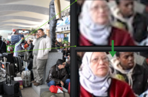
AI-based deep learning can also help in solving crimes if captured on CCTV cameras. Machine learning techniques can be used for colour conversion, regeneration, and comparison between two video backgrounds, which will help forensic teams to identify vehicles or objects during the post-incident investigation.

AI-based machine learning algorithms can help in other forensic activities such as:

  • Vehicle model detection
  • 3D face reconstruction
  • Video enhancement by Image Super-resolution
  • Video De-hazing and noise reduction
  • License Plate De-hazing
  • Predictive Image searching

Conclusion

Artificial Intelligence is the next evolution in Video Analytics. Owing to the advent of high-performance GPU hardware, Deep learning-based AI techniques are being widely adopted by various VCA software OEMs. This improves the detection accuracy without increasing the hardware cost exponentially. For end-users, it greatly reduces the workload of security staff and brings significant benefits by detecting unusual incidents and solving a lot of video forensic problems. Moreover, it enables them to use the massive amount of CCTV video data generated for system training purpose instead of getting overwritten over a period. In future, the quality of detection will continue to improve thereby improving the adoption of AI in Security and Surveillance.

This blog is a condensed version of the article titled “Role of Artificial Intelligence” published on “Security Link India”


Importance of Drones and UAVs in the Current Pandemic Situation

Drones and UAVs are unmanned aircraft with no on-board crew or passengers in it. They are pilotless vehicles that can either be remotely controlled or are pre-programmed for a specific mission (initially used for military purposes). Drones and UAVs predominantly includes the unmanned aerial vehicle, a remote controller, and a system of communications between them. Drones and UAVs were initially designed to fly for a long time at a controlled level of speed and height. Now, they come in various sizes and serve a multitude of purposes. Some Drones and UAVs are autonomous, while some are remote-controlled. Some are short flight drones while some are large, and which can operate for a couple of hours. Drones and UAVs can be designed for low flying and also made capable of scaling greater heights. The earliest use of Drones and UAVs dates back to 1849 when the Austrians used unmanned balloons loaded with explosives to attack the Italian city of Venice. With time the role of Drones and UAVs has evolved. They are now used in many applications – aerial survey, security and surveillance, and logistics.

Importance of Drones and UAVs in the current situation

With more than 21 million people infected with Drones and UAVs, Drones & UAVsCOVID-19 around the world, the coronavirus outbreak has made it difficult for human beings to live a normal life. Health authorities and other officials are finding new ways to handle the critical situation. While everyone is scared by the threat posed by the virus, local organizations have come up with new ways to help the people. The pandemic situation has brought in an unsurprising boom for remote technologies, virtual services, and business delivery systems to promote social distancing. One among them is the Drones and UAVs industry which has gained more and more popularity with its innovative solutions to help the public. In this blog, we address how drones are used to combat the pandemic situation.

Surveillance and Broadcast

The COVID-19 pandemic has brought in unprecedented Drones and UAVs, Drones & UAVssituations that are expected to have a long-term impact across the globe. To avoid the spread of the infection, authorities across the globe have limited mass gatherings in public areas. However, given the fact that we have to live with coronavirus, people will congregate for personal reasons and it is difficult to manage them using traditional surveillance methods.

Drones and UAVs provide an ideal solution in such situations. Police officials and other government authorities in many countries are using drones fitted with cameras to surveil streets, zones, and large public spaces and monitor the movement of every individual in the restricted area. Speakers are mounted on drones to broadcast messages and information about the lockdown measures, restricted zones, necessary precautions, etc.

Contactless Delivery

Since the COVID-19 virus is highly contagious,Drones and UAVs, Drones & UAVs human-to-human contact has to be minimized. To support the situation, Drones and UAVs are proving to be a valuable tool when delivering medicines and other essential items such as household goods, groceries, medicines, first-aid kit and also food to the local people who are either in red zones or restricted containment areas.

Aerial Spraying and Disinfection

Drones and UAVs have been used to spray disinfectant liquids on crops in a huge agricultural area. Since the novel coronavirus is transmitted via respiratory droplets and has the tendency to spread by touching contaminated surfaces, health authorities and government officials are using drones to spray disinfectants, to keep the public areas clean and prevent further spread of the virus. This method is much more efficient than traditional methods, as it covers large areas in a short time while minimizing exposure of health workers.

Temperature Check

As the world slowly accepts the fact that we need to learn to live with Coronavirus, more and more people are stepping out for their personal and professional needs. This poses a great challenge for governments and enforcement agencies in effectively monitoring and controlling the situation. Using the traditional methods of screening are mostly man-managed and have their own limitations. It is also challenging to check the infected individual in a huge crowd or public gathering. Drones and UAV Designs fitted with infrared cameras can be used to measure body temperature, check heart rate, and also detect when a person coughs in a crowd. They have the capability to scan multiple people at a time and provide real-time, accurate data for active monitoring, isolation, and control.

Conclusion

As the battle against COVID-19 continues, new versatile technologies are required to monitor and control the outbreak effectively. Drones and UAVs are proving to be a crucial tool during this pandemic and have immense utility, due to their unlimited potential and compact size. Several research organizations are working on setting up charging station in remote areas for automated drones to ensure a smooth operation.

Mistral offers custom designs for Drone Electronics for a wide range of Drones and UAVs. These electronics designs for Drones and UAVs can be managed via control apps through generic devices like tablets and mobiles. Mistral can help customer’s in designing Drones and UAVs and architecting sophisticated Drone Electronics with remote operation and real-time streaming of wireless HD video.

Embedded Applications Development – Blog

This blog aims at providing an insight into Embedded Applications Development and tools essential to developing an intuitive and user-friendly applications.

Embedded systems are growing smarter and intelligent across embedded domains. Thanks to the remarkable advancements in the field of electronics, especially wireless communication technologies, SoCs, Microcontrollers, FPGAs, networking techniques and cognitive computing among others that support ultra-fast communication and data exchange. The trend is spanning across the embedded landscape including automotive, industrial automation, semiconductor, consumer electronics, avionics, energy, and healthcare domains. While we talk about the explosive growth of embedded systems, we cannot ignore one significant factor that is fostering these advancements – Embedded Applications Development. Needless to say, embedded applications development, with their advanced features, intuitive and user-friendly nature are becoming key to any technological innovation in the modern era. We live in an era of no ‘NO’ to Apps. Apps impact Embedded Applications Developmentour day-to-day lives in one form or the other, more often through  the smart gadgets we use.
From the days when Apps displayed a myriad of data in a single window, Embedded Applications Development have evolved to presenting only the specific content or data the user needs. For instance, if we consider the data generated by an embedded system as a thousand-page book, modern-day apps help users by extracting that one paragraph which is relevant to the user, rather than showing the whole book. This blog aims at providing an insight into various types of Embedded Applications Development and the tools essential to developing an intuitive and user-friendly application.

Embedded Applications Development

IoT and Cloud Applications

IoT is disrupting several market segments, be it Industrial, logistics and supply chain, automotive, medical, smart cities and security among others. Connected fitness trackers, smart speakers, and IoT enabled building automation are already a common talk in the market. Embedded Applications DevelopmentFour key factors call for a developer’s attention when we talk about IoT App – The IoT device by itself, the data ingestion layer, analytics and finally the end-user. The data generated by the IoT devices are transmitted over a wireless or wired interface, processed and analyzed before being displayed at the user end. The data is presented in an easy to understand format, enabling the user to monitor, control and analyze the data and generate reports using an intuitively designed interface, which we call an IOT App or Cloud App based on the use case. An IoT app developer has to pay in-depth attention to various critical factors such as cross-device compatibility, interoperability, cloud integration, connectivity, scalability, data security, privacy and various standards & regulations. The developer should have expertise on a range of tools and techniques to develop reliable and robust IoT / Cloud Applications. Some of the tools for Embedded Applications Development or IoT Applications are:

  • IoT Analytics, cloud storage, web services using AWS / Google or other similar platforms
  • Communication technologies such as Cloud Connectivity, WiFi, WiMax, LTE, 6LowPAN, WirelessHART, ANT, ZigBee, BLE, NFC and RFID
  • Knowledge on communication protocols such as MQTT, CoAP, XMPP, DDS, STOMP, AMQP, REST, LWM2M, Websocket
  • Microservices and containerization

Web/PC Applications

Web/PC applications offer an intuitive interface for users to Embedded Applications Developmentcommunicate with embedded systems. Web/PC applications are advantageous in managing devices deployed in remote locations.  These applications communicate with the embedded device hardware over a low-level software code written typically in C. An HTTP request over the webserver carried out through the high-level program and the low-level coding communicates with the Hardware to trigger the command. As a developer one should have expertise on following tools and techniques to develop a robust Web/PC Application.

  • C, C++, BOOST, RabitMQ, ZMQ, Flat/Protocol Buffer for creating High performance, multi-threaded, Distributed Applications
  • HTML / CSS / CGI / python, PHP, GOLANG for optimizing Web pages / services for embedded low latency/footprint
  • HTML5, CSS 3, Sass, Bootstrap, Foundation, AngularJS, ReactJS, VueJS, NodeJS, Django, Flask, Laravel, Java for developing Enterprise Web applications
  • IoT Analytics, cloud storage, microservices using AWS / Google
  • Selenium, RTRT, gtest/cpptest for developing test automation software
  • Time-series Database, NoSQL database

Web/PC Applications are used in real-time distributed systems of Scientific, Engineering, Medical, Industrial, and Defense domains due to their evolving functionalities and remote management capabilities. Complex systems deployed in a demanding environment of extreme vibration, high temperatures, dust, etc. can be monitored and controlled with precision and accuracy using Web/PC applications.

Industrial Applications

Industrial Applications are widely used in a range of applications Embedded Applications Developmentsuch as Factory Automation, Oil and Gas, Mining and Industrial safety among others, to monitor and control complex systems and processes. Industrial Apps are integral to Industrial control systems, providing real-time analytics and intelligence to users, optimize production operation and thereby enhance productivity. These Embedded Applications can be implemented on various platforms including Industrial PCs, Tabs and Smartphones.

The spurt in robotics and automated machinery in an industrial environment coupled with the emergence of sophisticated Embedded Applications Development have redefined factory operations enabling remote monitoring, control, automated diagnostics, preventive maintenance while ensuring least downtime. Industrial Apps are widely used in Wearables, Manufacturing Control Systems, Warehouse & Inventory Management, Equipment Maintenance, Production & Workflow Management, Industrial Safety and security, etc.

Tool and Techniques expertise for Embedded Applications Development for Industrial domain  include,

  • Java and .NET for implementation of Industrial Apps
  • Microsoft’s SQL Server, ProgstreSQL, MySQL, DB/2, etc. for Database management
  • Analytics and Cloud Storage

Embedded Applications Development for Scientific and Medical Devices

As said in the beginning of the blog, even if an embedded device Embedded Applications Developmenthas all the required functionalities and features, it’s the UI that defines the user experience. Any medical/scientific product, be it a large system or a handheld device, demand an intuitive user interface, seamless user experience, feature-rich UI/UX controls and ergonomic design. Medical / Scientific Apps present complex data in a simplified and user-friendly format and help the users solve complex analytical challenges quickly and easily. Some of the popular tools used for the implementation of scientific apps are,

  • QT, UWP, Xamarin, C#, .Net, Electron for developing PC Apps
  • Report generation – Charts and Plots

 HMI Applications

Human Machine Interface or HMI is increasingly becoming a significant part of embedded systems. From data acquisition, communication, presentation to monitoring, Embedded Applications Developmentcontrol and diagnostics, HMI offers a safe and reliable interface for various complex industrial applications. Today, HMI is imperative to Automation applications as it forms the data foundation of the system. An HMI development activity calls attention towards three key things – a robust Graphical User Interface, memory optimization and power efficiency. Factors such as shrinking device size and increasing functional complexity are posing many challenges in creating intuitive, user-friendly designs. In addition, the spurt of graphics technologies across embedded applications is making a huge difference in our outlook towards HMI – as a user and a designer alike. HMI functions as a gateway between a multitude of hardware & software components in an Embedded System, which includes Hardware modules, I/O devices, controllers, servers, etc. For instance, in an industrial scenario, robotics controls in complex machines are enabled and managed through HMIs. Some of the popular tools used are Microsoft’s Visual Studio .Net, Qt/QML, Android, ReactNative, etc.

Mobile Applications

Embedded mobile applications are often designed for industry-specific use. Embedded Applications DevelopmentIn most cases, it complements a PC or Web Application, by enabling remote access to the embedded system. Embedded mobile apps are widely used in Industrial, Healthcare and Automotive industries. One of the primary concerns of Embedded Mobile Applications is security since these applications handle critical and confidential data over the internet. Implementation of a foolproof, secured App platform is critical to avoid any kind of data breach. Mobile devices are available on a wide range of processors and operating systems. Thus, the Application created should work seamlessly irrespective of the platform it runs.

Some of the popular tools to develop Native Android, iOS apps and Hybrid mobile Apps include,

  • Xamarin, QT for developing Hybrid Mobile Apps
  • Java, Kotlin, NDK, JNI (Android), ReactNative, Flutter for Android apps
  • ObjectiveC, Swift, ReactNative, Flutter for iOS Application
  • JustinMind, Adobe Photoshop/XD, Pencil, etc. for wireframes & prototyping

Bare-metal & Headless Embedded Applications Development

Bare-metal application is a firmware application, or a set of Embedded Applications Developmentsequential instructions executed directly on the system hardware – commonly on microprocessors or microcontrollers – and runs without an OS. Bare-metal applications are faster, are power efficient and use less memory. Due to these characteristics, bare-metal apps are widely used in time-critical, low latency applications that has stringent boot time but minimal CPU bandwidth, connectivity and memory; for example, DO-178 compliant applications for mission-critical and safety-critical systems. Headless Apps find its use in Embedded Apps Development for wearable, medical, home automation, industrial, health and wellness devices, wherein a user interface is not required for executing the functionalities. Some of the popular tools used for Embedded Applications Development for Bare-metal and Headless Apps include,

  • C/C++/Assembly apps on various IDEs for bare-metal environment
  • FPGA, DSP Algorithms

Conclusion

Apps have become an extremely critical element for embedded systems, be it consumer products, automotive, industrial, avionics, assistive, healthcare devices, scientific devices, drones, or any other systems that humans interface. Today, for every embedded product user, the system UI is, if not more important, as important the memory footprint or the overall system performance. It has become one of the key factors that decide the success of the product. Robust & flexible Embedded Applications Development is key to any embedded system – localization, screen size, resolution, failure scenarios, etc. need to be considered while developing an App. Mistral has over a decade of experience developing high quality, flexible embedded Apps for Display based and headless applications for Android, Linux, iOS and Windows-based platforms. Mistral’s comprehensive Embedded Apps development services include UI Customization, NDK Applications- Porting of Native applications to different platforms versions, QT/QML based UI applications, Media framework customization, Database and web-services, Cloud integration and Application porting among others.

IoT Testing Process for Building Robust IoT System

An IoT testing process to check the functionality of connected IOT devices. With the increasing acceptance of IoT devices there is an increasing need to deliver better and faster services. In this article, we will cover the various IoT testing process required to test connected IoT devices. 

Internet of things (IoT) as we all know is an ecosystem of systems, sensors and devices which are connected over a network enabling communication among them. IoT devices not only include computers, laptops, tablets, smartphones, but all the devices that incorporate chips that can connect to the internet to communicate and gather information. IoT is a platform which allows users to manage data and control the connected devices remotely. According to Gartner, approximately 8.4 billion things were connected in 2017, and the figure is expected to rise to 20.4 billion things by 2020. And, according to IDC, there will be 41.6 billion connected IoT devices, or “things,” generating 79.4 zettabytes (ZB) of data in 2025. The range of existing and potential Internet of Things IoT Testing Process, iot testing processesdevices is enormous.

With the current focus on smart cities, smart homes, and smart gadgets, it is expected that people, businesses, and the government will be tremendously impacted by IoT. Enroute to integrating more than 20+ billion devices into various verticals such as Agriculture, healthcare, smart homes, manufacturing, retail, etc., within the next few years, IoT development is expected to increase the scope of Internet of Things testing significantly. As the number of connected devices increases the challenges for software developers and testers also increases; so does the need for a defined IoT Testing Process. It is also expected that the smart devices such as coffee machine, toasters, toys, washing machine, automated smart doors, refrigerators, smart switches, and many others will be connected to the network and communicated via smartphones. All of these devices are enabled with either via Bluetooth, WiFi, RFID or Z-Wave to connect with each other seamlessly. Here are a couple of scenarios on how IoT could change your life:

Example 1 – When you return from a jog and park your bicycle in the garage, the sensors available inside the garage detects the opening of the door and sends a notification to turn on a coffee maker and microwave via IoT.

Example 2 – On parking your car in the allocated area of office space, the sensor sends the notification through IoT to turn on the air conditioner, cabin lights and enables a perfect start of the day.

IoT Testing Process helps to check the functionality of connected IOT devices. With the increasing acceptance of IoT there is an increasing need to deliver better and faster services. The thrust is to provide greater insight and control, over various interconnected IOT devices. Hence, IoT testing process is important and critical for development of IoT enabled Devices.

IoT Testing Process

In this article, we will cover some of the IoT testing process required to test connected devices. Before releasing any product in the market, it is of utmost importance to test the function of all devices according to the standards set for it. IoT systems, taking up the center stage in the consumer space, have to go through many important phases of testing. The IoT testing process for a product can vary based on the system/architecture involved. The IoT Testing process broadly revolves around Security, Analytics, Device, Networks, Processors, Operating Systems, Platforms and Standards. IoT product testers should concentrate more on the Test-As-A-User [TAAS] approach rather than following an IoT Testing process based on the requirements. Below listed are few components of the IoT testing process.

IoT Testing Process, iot testing processes

  1. End-user application testing

It is essential to ensure that all the connected devices such as smartwatches, automated doors, vending machines, industrial robots, etc., work seamlessly to provide a gratifying user experience. With a myriad of devices connected through the internet of things, usability testing becomes at most important.

  1. Security Testing

This is the top priority area in IoT testing process as all the devices are provided with IP addresses and can transfer data over the network. The spread of the IoT has been a boon for hackers who can easily target these devices. Hence, it is crucial to test all the devices to eliminate vulnerabilities and maintain the integrity and security of data. The prime area of focus in security testing includes data protection, device identity and authentication, data encryption/decryption and data storage in the cloud.

  1. Connectivity Testing

As all the devices in an IoT system are connected through the network, they must be available constantly and also ensure seamless connectivity with the user. There are chances of any of these connected devices going offline. Thus, it becomes crucial to check the behavior of the device during offline mode.  A warning message has to be sent to the end-user if the device is offline or does not have a unified communication with the user.

  1. Performance Testing

IoT devices continuously generate a huge amount of data. Performance testing ensures that these devices can work seamlessly without any interruptions. IoT performance testing is a complex and time-consuming process that ensures the development of a robust IoT system. This IoT testing process involves testing of multiple components and endpoints, network communication, internal computation, timing analysis, load testing, data volume, velocity, variety, and accuracy and scalability.

  1. Compatibility Testing

An IoT eco-system has a complex architecture as there are numerous devices which can be connected through it. All of these devices are configured with various hardware and software systems. This makes it important for a tester to perform a compatibility test between all the combinations of these connected devices to ensure seamless performance.

  1. Pilot Testing

Verifying the IoT system before the full deployment of the system is important as it helps the tester in identifying defects in the early state. In this IoT testing process, the entire system or a single component is tested under real-world operating conditions to check if it is ready for full-scale implementation.

  1. Regulatory/Compliance Testing

When it comes to IoT and IoT testing, regulatory and compliance challenges are likely to grow. In this IoT testing process, compliance of IoT applications for OFAC, HIPPA, GDPA, FDA, FCC, etc is determined. A regulatory test is done on the internal and external system to check if all the specified standards set by IEEE or W3C are met. The main objective of this test is to ensure that the system meets the standards, laws, policies, procedures, and guidelines after every development phase.

  1. Upgrade Testing

All the Firmware, Hardware, OS, Devices used in the IoT systems will need to get upgraded as the technology advances. So, it becomes important for testers to perform a thorough regression testing of all the connected devices in real-time before releasing upgrades to the end-users, keeping all the above IoT testing process in mind.

  1. Data Integrity Testing

Devices in the IoT system interact with each other and a lot of data exchange takes place. Hence, one of the aspects of the IoT testing process is to check the data integrity of IoT systems where the quality of data, accuracy, format, compatibility, and sanctity of data is tested. The data is validated from various devices, database, gateways and IoT servers.

Conclusion

IoT Testing Process can be different based on the system/architecture involved. An IoT system consists of Sensors, Applications, Network and Datacenters. Therefore, it becomes very important for the Testing team to determine the various type of testing required to test different IoT elements. And, depending on the system or architecture involved, the IoT testing process approaches might vary. It is very important for a tester to test the system using a Test-As-A-User (TAAS) approach, rather than testing based on the defined requirement. Using a TAAS approach helps to deliver a bug-free solution with improved UX to the end-user.

Mistral is a trusted IoT Service Provider, and over the past 27+ years, has offered a range of Internet of Things services to help you design and implement IoT device designs and IoT Gateway Devices to help realize your strategy. By ensuring interoperability, connectivity, scalability, and stability among various IoT components to form a healthy IoT ecosystem, Mistral, your IoT service provider offers a range of Internet of Things Services and IoT Testing Process that shorten the time-to-market for our customers.

SOC (Silicon) Validation Platform Development

Introduction

System on Chip (SoC) is becoming more and more complex in terms of functional capabilities, computing power, mutli-interface support and performance. SoC manufacturers strive to bring in as many features and capabilities as possible while scaling-down the Chip form-factor. This increasing complexity in chip design combined with faster time-to-market demands throw enormous challenges for Chip developers, which multiplies the efforts in SoC verification and validation. 

Verification, Validation and Testing are three important stages of Chip Development. It is crucial to have functional test platforms when the first pre-production sample of the SoC is out. Silicon Validation [SoC Validation] is often considered as the most critical phase of Chip development. It validates various attributes of an SoC such as power sequencing, reset and clocking schemes including boot mechanisms, and the SoC functional correctness. Further to this, the SoC release also has dependencies on power and performance parameters, thermal and electrical parameters, physical stress tests in a given environment. The features and functionalities intended to be achieved by the Chip need to be thoroughly verified and validated. The silicon verification, validation and testing processes consume the same amount of time or sometimes even more of the total chip development time. SoC validation is performed under aggressive schedules to meet time-to-market requirements. And this is where Test Platform developers play a crucial role by providing fully functional and validated test platforms before the actual silicon is ready.

The Test Platform development team develops the SoC Validation platform parallel to the chip development activity and ensure that the platform is ready by the time first silicon [Sample SoC] is out. This blog aims at providing a glimpse of SoC validation platform development and the validation processes at various stages of Chip development.

Typical Chip Development Flow

A typical Chip development process includes stages viz., Design Spec, Architecture design, RTL Design, Physical Design, Tapeout and Manufacturing. The Chip design verification happens during the chip development process. It’s crucial to have a clear roadmap for Chip release and Test/Validation Platform development, as the timely market release of a new Chip is dependent on its Validation.

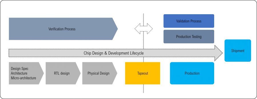
Fig: Typical Chip Manufacturing Flow

Silicon Validation Platform

Mostly SoC manufacturers deploy a different project team to work on Silicon Validation Platforms. Depending on the Chip Development Lifecycle and the complexity of the platform, Silicon Manufacturers may also employ an experienced Embedded design company to develop the Test Platform.

The figure below outlines various phases in the development of a Test Platform in cohesion with Chip Development activity.

Fig: Phases of Silicon Validation test platform development & Support

Pre-Silicon Phase

The SoC Validation Platform (SVP) design can start during the early stages of the SoC development itself. The Test Platform is designed in close coordination with the SoC design team. SVP developers seek various information on SoC such as the interfaces, SoC packaging, Power/Clock, end applications etc. from the SoC design team. This is to ensure that various features and functional capabilities envisioned in the SoC can be validated using the Validation platform.

Testing of Validation Platform

The complexity of the SVP increases with the complexity of the SoC. Hence, it is critical to validate the platform to ensure its robustness. The platform needs to be thoroughly tested to validate its functional correctness and performance before the actual SoC is available and debugged if any issues are noticed. This helps to minimize failures when the actual SoC is under test. There are several means to test a Validation platform.
Silicon Bring-up

A fully tested and functional Test Platform is used for Silicon bring-up activities. Typically, a Chip Manufacturer uses the actual fabricated silicon [Pre-production sample] to run the software and conduct the Silicon Validation Process. In this process, all functionalities and target use-cases of the chip are verified and validated. All major interfaces of SoC are functionally made available for verification on the platform. The process thoroughly analyses the performance of the SoC and tests the corners to validate the operating limits. The Test Platform development team is actively involved in the validation processes and supports the silicon team in setting up the system for checking out various boot modes and also the peripherals. The Test Platform development team also provides support in debugging failures if any are detected during the validation process.

Post silicon Phase

Silicon Validation is a continuous process and any functionality failures, bugs identified, or an upgrade required in the Test Platform is addressed in this phase. The Chip development team provides silicon samples to the platform developers to verify their findings. The Test Platform developers replicate these cases as applicable [Failures] and resolve the failure conditions.

The Chip Development team engages multiple line-ups to test various interfaces, peripherals, and functionalities at the same time. Test Platform Developers provide test suites and required documentation to ease out the initial setup and operation of the system. Once the Silicon/Chip is thoroughly validated with respect to all functional aspects, the chip Manufacturers team can proceed with the next phase of Silicon release.

Conclusion

Silicon validation is one of the crucial processes in chip release. It takes a palpable amount of time and effort to realize and implement a test architecture that meets all test requirements of a new SoC. In many instances, Chip Manufacturers depend on Product Engineering companies for the timely development of Silicon Validation Platforms. Mistral is an embedded engineering company having more than two decades of experience in collaborating with leading chip manufacturers in developing Test/Validation platforms, Evaluation Modules, Development Platforms and assisting them in successfully validating their SoCs. Mistral is one of the preferred design partners for Silicon companies. Mistral has in-depth knowledge on key components the validation processes that help chip manufacturers get their chips to market faster.

To know more about Silicon Validation and Test Platform Development Services, write to us info@mistralsolutions.com

In-flight Entertainment Solutions (IFE) – Evolution and Emerging Trends

What makes passengers air travel interesting? Window seats? Delicious meals and snacks? Or a full-fledged In-flight Entertainment solutions? Today’s generation of passengers crave for a great experience on-board which makes them feel satisfied and happy during their long-haul journey.

Today’s generation of passengers crave for a great experience on-board which makes them feel satisfied and happy during their long-haul journey. This is where in-flight entertainment  solutions play a significant role! IFE a key factor of the enjoyable passenger experience, is progressing as the technology advances. These advancements in technology have given birth to the era of “trickle-down in-flight entertainment” systems which has let airlines to provide benefits of premium entertainment content to their passengers. In-Flight Entertainment Design Services has evolved right from offering a traditional form of entertainment such as movie, music, radio for selected cabins to embedded seat-back In-flight Entertainment systems to every individual. In-flight Entertainment is one of the most exciting features in long-haul air travel, with most of the airlines equipping seats with seat-back screens or displays.

What is In-flight Entertainment (IFE)?

In-flight entertainment or IFE refers to the design & development of entertainment systems provided to airlines passengers. In-flight Entertainment Solutions can either be watching movies, entertainment channels, business, and news, listening to music or playing online games. In-flight entertainment solutions also facilitate and provide a wealth of information that could be of benefit to passengers, like, information on the travel route, onboard menu and procedural guidelines and other informative inputs. In-flight entertainment solutions have come a long way an occasional projector movie to sophisticated seat-back computers loaded with movies, games, maps, music and much more. IFE is often what gets many of us through the tiresome, long-haul flights. This service has been adopted by many airlines over the years and airlines are continuing to evolve & innovate new ways to keep the passengers entertained.

How has In-flight Entertainment industry evolved ?

The modern in-flight Entertainment solutions was born in the early ’60s when Trans World Airlines (TWA) installed a 16mm film system on a black and white TV monitors capable of holding the entire film, developed by David Flexer for the first time. Later, Avid Airlines product developed a pneumatic headset which was then absorbed by TWA. In-flight Entertainment, In-flight Entertainment Design Services, In-flight Entertainment SolutionsThroughout the early to mid-1960s, some in-flight movies were played back from videotape, using early compact transistorized videotape recorders, and played back on CRT monitors. These bulk-head displays in In-Flight Entertainment systems were commonly placed in the aisles above the passenger seats after every few rows. More than twenty monitors were installed in an aircraft, and passengers viewed movies on this unique closed-circuit system. This was an era far before the days of solid-state circuit boards and light-weight systems. In the late 1970s and early 1980s, CRT-based projectors began to appear on newer wide body aircraft, such as the Boeing 767. Some airlines upgraded the old film In-flight Entertainment solutions to the CRT-based systems in the late 1980s and early 1990s on some of their older wide bodies. In 1988, the Airvision company introduced the first in-seat audio/video on-demand systems using 2.7 inches LCD technology which were run by Northwest Airlines on its Boeing 747 fleet. It received overwhelmingly positive passenger reaction and as a result, it completely replaced the CRT technology.

Current In-flight Entertainment Solutions

The advancement in the Consumer electronics industry with smartphones and display technologies had made the display screens get thinner & lighter. This revolutionized the In-flight entertainment solutions and lead to the concept of personalized screens for each passenger. In the past decade, as Android became the mainstream of technology life, airlines and in-flight entertainment solutions OEMs started to migrate their in-flight entertainment system to run on Android. According to Virgin America, “using Android makes the system easier to maintain and upgrade”. With Android-based in-flight entertainment solutions, passengers will be able to play games, watch movies, listen to music, order meals right from their comfort seat.

Many ODMs and product development companies offering In-flight Entertainment Design Services also provide support for USB ports, audio jacks, and a credit card reader. The current In-flight entertainment solutions consist of a crew control system, seat-back display units, the system and content server, satellite antenna, infrastructure components, the Wi-Fi in the aircraft, the data and power cabling and the wireless access points to link to passenger’s personal electronic devices.

Key design criteria for any In-flight Entertainment system includes system safety, cost optimization, software reliability, hardware maintenance, and compatibility with user devices. The current decade’s innovations have focused on customizing In-flight Entertainment Solutions to suit passenger needs. A sharp trend shaping the travelers In-flight Entertainment experience is the option to plug-and-play with their own devices. The latest In-Flight Entertainment solutions with Android-based architectures are fully scalable and highly customizable. It enables passengers to make payments through secured apps, order services via apps and also enjoy a wide range of entertainment applications.

 Features of In-flight Entertainment Solutions

In-flight Entertainment Solutions can provide various features for different parties such as airline companies, cabin-crew members, and passengers. These features are enabled through software and hardware components. The In-flight Entertainment systems also create a dynamic link between passengers and crew members.

  • Audio and Video in In-flight Entertainment

The next-generation In-flight Seat Video Display unit provides passengers with access to broadcast video programming, navigation through menus, browsing web pages and access to Video-on-Demand (VOD) and Audio-on-Demand (AoD). Some airlines provide personal televisions (PTVs) for every passenger with channels broadcasting new and classic films, as well as comedies, news, sports programming, documentaries, children’s shows, drama series, video games as part of the video entertainment system.

This can be customized for each passenger, who can watch the program of their interest on the Seat Video display unit. A passenger using the in-flight entertainment system can also enhance the PTVs service by using subtitles of the running dialogue, along with the details of the characters. This special service helps viewers who have hearing difficulties. Furthermore, they can be written in a different language to help people who cannot understand the spoken dialogue.

  • Air Maps

The air map in an in-flight entertainment solutions provides passengers with up- to- date information about their travel. It has become the most popular element of IFE systems, capturing passengers’ attention by posting live updates about their journey. In addition to displaying the position and direction of the plane, the map also displays the altitude, airspeed, outside temperature, travel distance travelled, elapsed time, and remaining time to give passengers the sense of movement.

  • E-magazines

At the outset, all the airlines provided a free paper-version of a magazine to all their passengers which were placed at the seat-back. Most airlines are now distributing their magazines digitally via tablet and other software applications. These e-magazines are not limited to just text; they provide various information either in the form of video or images. Some airlines also provide e-books as a value-added feature to their systems. Using an electronic version of printed media can change their importance by adding interactive features such as e-commerce services where a passenger can choose his products and buy them instantaneously.

In-flight Entertainment Trends

The future and growth of In-flight entertainment Design Services depend on several factors. The need to enhance the passenger experience, technological developments and an increase in aircraft deliveries with advanced In-Flight Entertainment solutions are factors expected to drive the market. However, the regulatory framework and certification and an increase in the overall weight of aircraft are expected to restrain the growth of the market. The need for personalized entertainment has contributed to the increasing demand for In-Flight Entertainment design services. Various airlines are competing with one another to keep up with the continuously evolving expectations of passengers.

  • Wireless In-flight Entertainment

In-flight Entertainment, In-flight Entertainment Design Services, In-flight Entertainment SolutionsWireless IFE is a wireless content distribution system to passengers’ devices. The Wireless IFE systems are light-weight compares to the traditional conventional In-flight Entertainment Solutions. Most passengers favor their own devices for inflight entertainment.

Besides, the wireless IFE systems allow hassle-free internet access, browsing, video streaming, and more on passenger’s devices. Airlines are also jumping on the BYOD (Bring Your Own Device) bandwagon and replacing their existing In-Flight Entertainment solutions by turning passengers PEDs into a comprehensive entertainment solution.

  • WiFi and Connectivity

Various airlines services have installed routers to provide free Wi-Fi to their passengers. In several aircraft, data communication via satellite system allows passengers to connect to live Internet from the individual IFE units or their laptops via the in-flight Wi-Fi access. Using Wi-Fi, passengers can access movies, music, games and other entertainment media from their own devices and enjoy their journey.

  • Consumer VR

Most of the airlines and ODMs are now looking at IFE devices that offers Virtual Reality entertainment experience on-board where a passenger can just pop on the immersive glasses and watch movies or play games. These immersive headsets present a viable way of improving passenger comfort and satisfaction.

Conclusion

Technological advancements in consumer electronics have contributed to the development of advanced IFE systems to enhance the passenger experience. For instance, Virgin America is presently testing the new EcoV2 monitors developed by Panasonic. Various airlines are collaborating with In-flight Entertainment Solutions manufacturers to introduce jazz seat concept that offers several benefits such as improved touch sensors and display, integrated passenger control unit, and programmable attendant call buttons. With the increasing frequency of travel and the number of options available, the passenger will be more discerning in choosing an airline. Airlines will have to differentiate on the quality of experience they offer to passengers and IFE systems and in-flight entertainment design services will play a crucial role.

Passengers will expect the In-flight entertainment Solutions to provide them with the same experience as their smart devices. It is imperative for the suppliers of these systems to consistently innovate and keep pace with emerging technologies, to stay ahead. By combining creativity, technical expertise, and refined processes, Mistral offers cutting-edge embedded hardware and software design services or In-flight Entertainment Design Services, home/ automotive infotainment solutions to ODMs. Our in-flight entertainment design services keep up with the latest trends and include seat-back and portable IFE units that integrate audio, video, wireless technologies and DSP Algorithms and HMI paving the way for intelligent, connected in-flight entertainment solutions.

Trends in Medical Electronics

As technology evolves, OEMs are widely exploring the scope of adopting the latest technology trends to Medical Electronics. Trends such as Artificial Intelligence, Augmented/Extended Reality, Internet of Things etc. are set to have an enormous impact on the health-care industry. Here are some of the recent Trends in Medical Electronics that are expected to have a huge impact on the segment:

Wearable gadgets – The modern-day innovative, secure, and highly efficient wearable devices are helping people to maintain their daily routines, keep track of their health and be more aware of their health.

Wearable devices such as smartwatches, activity trackers, health monitors etc. come equipped with sensors to help users monitor heart rate, BP, Glucose, weight, SPO2, etc., while maintaining the log of such parameters. This data can optionally be shared with the physicians thereby contributing significantly to a person’s well-being.

Blockchain Systems – Blockchain systems work like Electronic Medical Records (EMR), where the patient’s health record information is digitally stored on the cloud with minimal space consumption. The Blockchain technology allows a patient, physicians or any trusted users to faithfully and securely access or share the information remotely. Using this, patients can easily connect to multiple hospitals and collect their medical reports automatically and a physician can have a look into the history of the patient’s medical reports and provide an accurate diagnosis, along with effective and cost-effective care.

Telemedicine – The modern medical applications both wired and wireless are making the life of patients, especially the elderly and physically challenged, easier by allowing them to consult and get prescriptions from doctors on their smartphones. The doctors can also remotely monitor the patient’s health and make diagnosis and treatment decisions quickly.

Artificial Intelligence (AI) – Artificial Intelligence is set to change the health-care industry in many ways. AI-based devices can process information with speed and accuracy and help doctors provide a diagnosis or create a treatment plan. Design of BOTs (using AI/ML/DL) are underway to assess and diagnose the medical situation/circumstance and prepare report/plan/suggestion to assist the medical/paramedic personnel.

AI along with Machine Learning(ML) can be used to explore chemical reactions in the drug industry, digitise medical records, schedule appointments online, help surgeons offer deep insights on the surgery, interpret multiple data sources at the same time from different variables, provide enhanced treatments in cases such as radiology and more. AI is helping the health-care industry to transform from traditional treatment into targeted treatments and personalised therapies.

Internet of Things (IoT) – Internet of things is one of the rapidly growing technologies which has opened a world of possibilities in the healthcare industry. Internet of Medical Devices (IoMT) helps in real-time monitoring of the patient and notifying the physicians by means of smart medical devices connected to a smartphone with accurate data for early treatment. The IoT based medical devices such as glucose monitor, insulin pens, blood pressure monitors, etc are among the most used medical devices at homes and in hospitals to monitor and provide real-time information to doctors for quick and accurate diagnosis and treatment.

Extended Reality – The technology which is assumed to be purely for gaming and entertainment is now healthcare. According to Goldman-Sachs report, the AR/VR healthcare market would reach a total of $5.1 billion in 2025, with an estimated 3.4 million users throughout the world. Virtual reality is helping patients with memory, visual impairment, depression, etc., with vivid imagery provided via headsets that acts as a mode of distraction or a way to avoid or lessen the pain medication. Augmented Reality helps provide another layer of support for medical practitioners and aid physicians to visualize obstacles before complex surgeries. The Mixed Reality, a mixture of the virtual and real-world, is used to educate the healthcare practitioners, medical students and professionals to understand the condition of the illness and explain the treatment to the patient.

Conclusion

These are just a few of the technologies that are being adopted by the healthcare industry. As technologies evolve, the way healthcare providers interact with patients and deliver care is also changing and the healthcare and medical electronics industries are about to witness a lot more significant changes in the upcoming years.

Read our blog on “An Overview of Medical Electronics” to know about medical electronics and its types.

An Overview of Non-Invasive Medical Electronics

Non-Invasive Medical Devices cater to not just solution specifications and functions to satisfy users’ needs but addresses healthcare regulatory compliances. This blog provides a comprehensive an overview on the various types of Non-Invasive Medical Electronics currently  in use.

Introduction

In today’s world, technology plays an important role in every industry as well as in our personal lives. Needless to say, medical and healthcare is one of the domains where technology is playing a crucial role. The integration of the latest technologies and several scientific innovations in Non-Invasive Medical Devices development is hugely enabling the healthcare industry by providing cutting-edge Medical diagnosis and treatment procedures, saving countless lives across the globe. The advancements in Non-Invasive Medical Electronics has introduced miniaturization and enhanced applications, specifically in the areas of medical data acquisition, storage, and analysis. These advancements in Non-Invasive Medical Electronics are aiding physicians in quick diagnosis, continuous monitoring, and providing better treatments. One of the reports from Markets and Markets shows that the estimated medical electronics market in 2019 was USD 5.1 billion and the study projects it to reach USD 6.6 billion by 2025, at a CAGR of 4.6%.

What is Medical Electronics?

One of the most extensively growing fields in today’s era is the Medical Electronics or Medical Electronics Devices. “Medical Electronics” is the study of electronic Non-invasive Medical Electronics, Non-invasive Medical devicesinstruments and devices that are used for diagnosis, therapy, research, surgery, monitoring & analysis of the patient’s health. Medical Electronics is a perfect amalgamation of embedded systems, software applications and medical science to improve healthcare services. With embedded technology, the physicians can obtain the medical reports of the patient instantly, view them on embedded software-driven electronic devices, monitor the patient, and give consultation remotely without any hassle.

Non-Invasive Medical Electronics Devices

Medical Electronics Product Development constitutes a wide range of medical devices, which can be classified into two categories, namely – Invasive Medical Devices and Non-invasive Medical Devices. Medical devices such as an endoscope, Cardiac Pacemakers, and Biosensors, laparoscope that break through the skin or inserted through a body cavity (nose, mouth, etc.) to screen, analyze or support one or more body functions are termed as Invasive Medical Devices.  Vital sign monitoring devices such as ECG, Glucometer, Digital/IR Thermometer, Digital Stethoscope, and imaging devices such as MRI, CT Scan, and other life support medical devices, used in diagnosis and treatment without penetrating the body are termed as Non-invasive Medical Devices. Many of these non-invasive medical electronics are nowadays available in compact form factors and support regular or continuous monitoring at home.

Types of Non-Invasive Medical Devices

Medical device product development is the process of turning a medical device concept into a commercially viable product. Medical devices requires specific stages to be followed to ensure design control so that the product is both effective and safe for use. As a result, this covers the entire product development cycle, from medical device design to clinical trials, and risk management to manufacture. Some of the Non-invasive Medical devices can carry an inherent risk as these devices may impact the health of patients. Thus, the process of medical device design and development has to adhere to regulations, specifications and user requirements to ensure that the device safe and effective for commercial application. Listed below are a few of the popularly known non-invasive medical devices .

CT Scan and MRI – Computed Tomography (CT) scanners and Magnetic Resonance Imaging (MRI) are medical imaging techniques used in radiology to non-invasively scan the body. CT Scan uses X-rays to scan the body part from different angles and produce the cross-section images whereas MRI scanner uses strong magnetic fields and radio waves to generate a detailed image of soft tissues and bones of the body. Both the scanners are painless and help the physician to diagnose issues w.r.t bone fractures, tumours, cancers, etc., without breaking through the skin. They provide detailed information about the condition of the patient to the doctors.

ECG – Electrocardiogram (ECG) is an Non-invasive medical devices that monitors the activities of the heart and provide full disclosure Non-invasive Medical Electronics, Non-invasive Medical devicesECG signal, complete data, analysis as well as comprehensive reporting of the patient’s condition. The electrodes are placed at various points on the patient’s torso and the sensor detects the electrical activity of the heart, records the electrical signals, and displays the comprehensive data on the digital screen. There are various types of ECG machines right from the large 12 Lead ECG machine to handheld, wireless ECG. Medical device design and development like wireless ECG, enable the result to be shared with the doctor for supervising the heart rate variability of a patient, remotely.

Electronic Fetal Monitoring (EFM) Machines – During pregnancy, labour, and delivery of the baby, the heart rate of the baby, maternal uterine activity such as the strength of the uterus and the duration of the contractions of the uterus is monitored to help the physicians assess Fetal well-being before and after labour. The medical device design and development and related Medical Device Software Development of these machines consist of a monitoring unit, cables, electrodes and algorithms to measure record and display the Fetal Heart Rate (FHR), uterine contraction, maternal BP, and heart rate during delivery.

Defibrillators – Defibrillators are used by physicians to monitor a patient suffering from cardiac issues. The defibrillator analyses the patient’s heart for inconsistent rhythms and restores a normal heartbeat, when necessary, by gently sending electric shock. They are also used to restore the heartbeats of a patient if the heart suddenly stops functioning.

Glucometer: A portable device to check the blood sugar Non-invasive Medical Electronics, Non-invasive Medical deviceslevel of the patient. The wireless smart glucometer measures the glucose levels in the blood and displays them on smartphones. It is a technique where the lancet lightly prinks the skin to obtain the blood. The device detects the glucose concentration in the blood and converts into a voltage using special sensor strips. The current flowing through the circuit provides a measurement of the concentration of hydrogen peroxide, displaying the glucose concentration on the digital screen or sending it to a smartphone.

IR thermometers – The Infrared (IR) thermometer, sometimes called Laser thermometers is used to help aim the thermometer for measuring the temperature of a patient from a distance. The thermometer includes a lens to focus the IR thermal radiation on to a detector, captures the radiation, and converts it into an electrical signal and displays in units of temperature on the compact screen.

Digital stethoscope – A palm held stethoscope is the smallest and most powerful and comfortable device which uses audio headphones to hear the heartbeat. It has a microphone in the chest piece which allows a doctor or clinician to accurately understand the pathology behind the heartbeats. It can convert an acoustic sound to electronic signals and amplify it for optimal listening. These signals can be digitized and transferred to either laptops or computers for diagnosis.

Blood Pressure monitors Non-invasive Medical Electronics, Non-invasive Medical devicesBP monitors can either be placed on the upper arm or wrist. The sensors present in the device detect the arterial wall vibrations, converts the analog signals to digital, and display the result on the LCD screen.

Blood Oxygen Monitor – SPO2 or Pulse Oximeter, this device estimates the amount of oxygen in a patient’s blood. It is a painless process of emitting and absorbing an infrared light wave passing through the capillaries of fingertip, toe, or earlobe. A variation of the light wave passing through the blood vessels (or capillaries) is used to determine the SPO2 level and the result is processed into a digital display of oxygen saturation on the monitor.

External cardiac pacemaker – The pacemaker is a small medical device that is used to treat arrhythmia. The device is placed on the patient’s chest to maintain an adequate heart rate. It generates electrical pulses delivered by the sensors called electrodes which detects the patient’s heart rate and accelerates it to contract and pump the blood when the heartbeat is abnormal. The modern pacemakers are extremely programmable and are expertise in optimizing the pacing modes for individual patients. The modern pacemakers can also monitor the blood temperature, breathing, and adjust the heart rate with changes to the activity of a patient. Many of the above mentioned non-invasive medical devices are available in multiple formats and also support home health care and remote monitoring. Some of these store data in the cloud and the information is accessible to doctors to provide continuous monitoring and guidance to the patients.

Conclusion

The non-invasive medical electronics industry has advanced to the extent that individuals can now monitor their health at home using sophisticated equipment. With the bloom of Industry 4.0, Internet of things, Artificial Intelligence and Medical Device Software Development, the future looks great for non-invasive medical electronics. Read our blog “Trends in Medical Electronics” to know more about the impact on these technologies on Medical Electronics.  Mistral has extensive expertise in design and development of non-invasive medical devices that support and aid medical professionals in data acquisition and communication. Our experience in AR/VR designs and IoT along with expertise in a broad range of platforms, Mistral brings invaluable processor/operating system/testing/ system validation expertise to the medical device design and development process. The non-invasive medical electronics team at Mistral facilitates medical product development through all phases – from initial concept generation to proto manufacturing and production support. Mistral’s medical device product development team also offer medical device software development including integration of medical sensors, porting, and application development.

Recent Trends on RF Data Converters

Overview

Analog to Digital Converters (ADC) and Digital to Analog Converters (DAC) act as a bridge between the Analog and Digital Domain. For years, these devices have remained the interface between analog and digital world. However, in higher Radio frequency (RF) range (Giga Hertz), the speed offered by ADC/DACs becomes a bottleneck.

The Traditional Approach – Heterodyne Conversion

Here’s a quick look into how an ADC/DAC is using in the traditional approach. An input RF signal is down converted to an Intermediate Frequency known as IF. The carrier wave is shifted to IF as an intermediate step by mixing the signal with a local oscillator. Once the signal is in IF range, simple analog circuits are used to filter, fine tune and amplify or attenuate the signal as required. Such processed analog signals are then taken to the digital world through ADC for digital signal processing.

Similarly, in Digital to Analog conversion, the processed signal data is taken from digital world to Analog world through DAC, and from IF to RF through UP Convertors. This approach is called Heterodyne Conversion (IF)

A typical Radio Receiver design based on Heterodyne Conversion (IF) is shown in Figure 1.

Figure 1

The modulated RF carrier is passed through a low-noise amplifier (LNA) and a band-pass filter (BPF) before converting to IF as shown in the Figure. After passing through anti-aliasing filter (AAF) the IF is digitized by ADC. Demodulation is carried out at baseband level.
The above approach is mostly due to the limitation of the conversion speed of ADCs. If we were to break the ADC speed barriers, would it be feasible to think of direct sampling?

Now, let’s look at the transmitter path for Heterodyne approach. Here, the baseband data is modulated in the digital domain & applied to DAC to convert to IF. The IF is upconverted to RF using a mixer & LO as shown in Figure 2.

Figure 2

Direct Conversion or Zero IF

Direct Conversion or Zero IF is an alternate to Heterodyne (IF) approach of handling RF signals using High-speed RF ADCs. In this, the RF carrier is down-converted directly to baseband instead of IF. The RF carrier is converted to baseband (I&Q) using IQ mixer as shown in Figure 3. Two ADCs are used to digitize I&Q data. Here too, demodulation is carried out at baseband level.

Figure 3

RF ADC

New high-frequency ADCs known as RF ADCs can directly sample wideband signals beyond 6.0GHz. In addition, these RF ADCs have built-in signal processing capabilities. An RF system designer, using the latest RF ADC, needs to design only the hardware platform and use software to configure the hardware to suit the application. An RF ADC with signal processing capabilities is shown in Figure 4.

Figure 4

Now, let’s look at the transmitter path. The baseband data is modulated in I&Q modulator and applied to two DACs, which is further upconverted to RF using IQ mixer and LO as shown in Figure 5.

Figure 5

RF DAC

The high frequency DAC, known as RF DAC, can generate frequency up to 6GHz directly, thereby eliminating the need for IF to RF conversion. RF DAC includes signal processing as shown in Figure 6.

Figure 6

Conclusion

Zero IF systems reduce component count and complexity of the design and bring in a lot of advantages. The System Noise Factor is minimised, and the out-band RF blockers can be attenuated by the RF front-end filters. Overall Zero IF systems are compact and provide better performance. At the same time, since High-speed ADCs are new in the market and expensive, a cautious approach is required before finalising the design.

The trends for Zero IF systems are further moving towards System on Chip concept. High-speed ADCs and DACs integrated with programmable logic eliminate the need for complex digital interfaces between converters and digital circuit. Such devices can be placed with the antennas and digitally interfaced to the processing world.

ARM Technologies and its significance in Embedded Domain

The ARM architecture based design, also known as the big.Little Design, is a heterogeneous multi-processing system that uses more than one processor core and offers multiple software architectures like AMP Architecture based Designs, SMP architecture based Designs and HMP Architecture based Designs.

We encounter many embedded systems every day in our life, starting from smartphones and tablets to computers, Medical devices and other electronic gadgets that provide high-computing capability. These electronic systems need to handle diverse compute requirements, and diverse workloads and are not industry-specific; they span across several markets. In the 1980s, Acorn Computers developed the first ARM processor at Cambridge University, England for commercial purposes. AMP architecture based Designs, big.Little Design, HMP architecture based Designs, SMP architecture based Designs
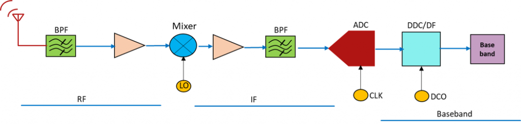
These ARM processors were further enhanced to provide high-performance and efficient power management without disrupting the system’s overall efficiency.  Microprocessors are astounding devices. They integrate the brain of a computer onto a single electronic component. The computing power that once required a room full of equipment now fits onto a razor-thin slice of silicon. Due to their compact size, microprocessors are now widely used in the silicon industry to design electronics products with the processor as the core of the system. Processors are categorized based on their internal architecture.

What is ARM?

The two most popular architectures are:

  • CISC (Complex Instruction set computing)
  • RISC (Reduced Instruction set computing)

CISC stands for Complex Instruction Set Computer is a CPU design strategy that uses a minimal number of instructions per program, forfeiting the number of cycles per instruction. For example, load data from the memory, perform an arithmetic operation, and store data back in the memory are the instructions of a single program that are performed in one single step. This is used in laptops, PCs, etc. to execute heavy graphics for games, perform complex math computation etc. RISC (Reduced Instruction Set Computer) is a CPU design strategy where few basic operations are divided into a small set of instructions within a single CLK cycle, enabling it to operate at higher speeds. For example, load command only loads the data, and store command only stores the data. Based on the application RISC and CISC architectures have their own advantages. ARM (Advanced RISC Machines) is a popular RISC architecture, which is a ubiquitous name in the processor industry. Because of its reduced instruction set, and fewer transistors, it is widely used in modern devices that need high computing capability with power efficiency. ARM is the heart of advanced digital products like routers, printers, smartphones, tablets, digital cameras, medical devices, robots, home appliances, wireless communication technologies, and many more.

ARM Architecture (big.Little Design)

The ARM architecture, also known as the big.Little Design, is a heterogeneous multi-processing system that uses more than one processor core. The “big” processor cores are used to render higher levels of performance within the thermal design boundaries, while the LITTLE processor cores are used to achieve power efficiency. The big.LITTLE Design clubbed with ARM architectures like AMP architecture based Designs, SMP architecture based Designs and HMP architecture based Designs enable the creation of devices at every level and allows these devices and applications to work robustly and efficiently and at the same time provide significant performance.

Let’s consider ARM Cortex-A9 as an example. While choosing a processor, the application that one intends to implement forms a major factor in the decision. Many applications require processors that are highly power-efficient and with high compute capability, e.g. smartphones and tablets. These applications are most often based on battery-operated devices. As the battery technologies have not kept pace with processor technology, there is an impetus to produce different types of processors that are power efficient to overcome the lag in the battery technologies. The requirement of efficient power management has led to the evolution of the concept of big.Little Design, a combination of power-efficient operation and yet having the significant computational capability.

Processors with ARM architectures are constructed with cores that share the same instruction sets but have micro-architectures that are optimized for either power or performance-related requirements. The ARM Cortex-A9 is a 32-bit multi-core processor which is based on the big.LITTLE Design providing four cache-coherent cores. The multi-core processor is built to deliver unprecedented heterogeneous multi-processing capability along with low power consumption that enables products in a wide range of new and existing ARM markets ranging from mobile computing, high-end digital home entertainment, automotive infotainment, in-flight entertainment, servers, and wireless infrastructure among others.

The Cortex series is one of ARM’s most widely deployed applications processors, which makes it suitable for low-power, cost-sensitive, 32-bit devices that require competitive performance. The introduction of big.LITTLE Design by ARM provided the industry with a breakthrough in power to performance ratio, which was lacking in the general Processor Silicon industry. With multicore embedded systems becoming so common, this part of the article outlines the possible multi-processing architectures. Broadly, there are three options: Asymmetric Multi-Processing (AMP architecture based Designs) and Symmetric Multi-Processing (SMP architecture based Designs) and Heterogeneous Multi-processing (HMP architecture based Designs).

Types of ARM Software architectures

  1. HMP architecture based Designs

The most powerful and complex system model for the big.Little Design is the Heterogeneous Multi-Processing (HMP). HMP architecture based Designs combine several different types of multicore processors, which enables the use of all physical cores at the same time. In HMP architecture based Designs, different processing elements perform different types of functions simultaneously. Threads with high priority or computational intensity can, in HMP architecture based Designs, be allocated to the “big” cores while threads with less priority or less computational intensity, such as background tasks, can be performed by the “LITTLE” cores. One of the best example of HMP architecture based Designs are wearable devices like a smartwatch with rich GUI.

  1. SMP architecture based Designs

Current multi-core processor technology has multiple instances of processing cores within a single device. These cores are tied to a single memory and internal system management. When you have a big.Little Design program to execute, the processor divides and shares the threads among all processors to work in tandem and provides Symmetric Multi-processing. In SMP architecture based Designs, the throughput of the system is increased. Also, programming and executing the codes in SMP architecture based Designs are comparatively simple because the program can be divided into multiple threads and any thread can run on any processor core and achieve approximately the same performance.

  1. AMP architecture based Designs

Asymmetric Multiprocessing (AMP) or AMP architecture based Designs is a contrast to Symmetric Multiprocessing. In AMP architecture based Designs, there is a single master processor that hosts the OS and controls all the tasks. In other words, AMP architecture based Designs have a master-slave relationship, where a master processor allocates the thread to all the slaves’ processors and controls the I/O processing and other system activities. The processors are not treated equally in AMP architecture based Designs, as the task handled by each processor is different and takes its own time to execute.

For instance, a processor may handle only I/O related operations whereas other processors may handle only OS codes. AMP Architecture based Designs are most likely to be used when different CPU architectures are optimized for specific activities – like a DSP and an MCU. In an AMP architecture design, there is the opportunity to deploy a different OS on each core – e.g. an RTOS and Android/Linux – as needed for the specific application.

Why ARM Technology and processors got popular?

ARM Holding is a leading company that was found in the 1990s. It offers a family of reduced instruction set computer (RISC) architecture which is designed specifically to form the cores of processors. This core design is licensed to silicon companies who can incorporate the processor core in their IC design in an efficient, affordable and secure way. ARM enabled AMP architecture based Designs, SMP architecture based Designs and HMP architecture based Designs aid creation of devices for all types of applications, with a complete toolkit and a strong global ecosystem for support. They provides a set of rules to the silicon companies which describe how the hardware works when an instruction is executed.

The ARM architecture is used on CPUs to run applications software, with platform security machine to secure trillions of connected devices, and embedded systems, and thereby help the ecosystem to design secure and efficient systems as easily as possible. ARM’s comprehensive product offering includes 32- and 64-bit RISC microprocessors, graphics processors, enabling software, cell libraries, embedded memories, high-speed connectivity products, peripherals, and development tools. Due to low power consumption and high performance, ARM processors are being used in most of the modern devices. They have gone through several iterations to increase performance and improve power efficiency. This combination of high performance, low power consumption, wide offering, and low cost makes ARM processors popular. ARM processors have been providing better performance when compared to other processors. It is very easy to use ARM for quick and efficient application development and hence it has gained huge popularity in all varieties of applications.

Here are a few of the advantages of ARM processors and their big.Little Design that have made them popular in modern-day electronics.

  • They offer a variety of software system models like AMP architecture based Designs, SMP architecture based Designs and HMP architecture based Designs
  • They offer a cost advantage compared to other processors
  • They are designed to consume less power making it ideal for a wide variety of portable and battery-operated devices.
  • Each core performs one operation per cycle and thus work faster
  • The availability and applications support offered by ARM has also helped in popularizing the ARM processors

Automotive and Infotainment Technologies – An Overview

Automotive Infotainment or In-vehicle Infotainment (IVI) is the integration of hardware and software system which delivers information and entertainment to driver & passengers through various on-board electronics and applications. Over the last decade, there has been a massive growth in the field of “Automotive and Infotainment” which is expected pursue between 2019 to 2028.

Automotive Infotainment systems or In-vehicle Infotainment can be termed as high-end radios that are far more more integrated. Automotive and Infotainment systems bring together telematics, information and driver-assistance features to create a unified in-vehicle experience. The primary driver for this integration of Automotive and Infotainment systems is the need for an improved driver experience, with both safety and cost playing a crucial part. The evolution in customer experiences with personal devices and gadgets are shaping expectations for automotive and infotainment systems making it a fast-evolving segment of the automotive industry. In the current day scenario, in Automotive and Infotainment applications consumers expect entertainment, connectivity and seamless access information and content from a variety of sources. This increase in in-vehicle or Automotive Infotainment solutions is fueled by an increase in customers’ focus on comfort and the growing trends towards electric vehicles, driver assistance, and autonomous cars. Automotive and Infotainment, Automotive Infotainment, in-vehicle infotainmentGone are the days when buying a car with only a music player was lavish. The time for automotive and infotainment has changed!

According to Markets and Markets, the Automotive and infotainment market is projected to reach USD 30.47 Billion by 2022, at a CAGR of 11.79%, whereas Mordor Intelligence predicts that Automotive Infotainment system market is expected to register a CAGR of 12.29%, during the forecast period, 2019-2024. Today, the automotive and infotainment technology is evolving rapidly, and everything is getting automated. Vehicles with enhanced safety, security, comfort, performance, availability and automotive infotainment systems are in high demand. Users are enthusiastic to own a vehicle with highly integrated communication, information, and entertainment systems (Automotive and infotainment systems) that connect all their smart devices and gadgets and provide them a seamless experience. The cockpit of an Automotive Infotainment system requires advanced processing capabilities to meet consumer demands for connectivity, safety, and future mobility.

What is Automotive and Infotainment ?

Automotive and Infotainment, also known as In-vehicle Infotainment (IVI) has become an important part of vehicle electronics. Automotive infotainment systems are a combined hardware and software solution that delivers streaming audio and video within the vehicle. It is the integration of hardware and software system which delivers information and entertainment to the driver and passengers through various on-board electronics and applications. The simple automotive and infotainment system which originated a few decades ago incorporated a car audio system consisting of FM Radio and CD player which could be operated using a simple dashboard knob.

As technology evolved, In-vehicle Infotainment systems in vehicles were equipped with dashboard cluster, display and touchscreen, text-to-speech and voice recognition to provide drivers on-board with exclusive user experience. The latest in-vehicle infotainment or Automotive infotainment systems also provide audio control and call pick-up functionality on the steering wheel ensuring smoother operation and a minimal distraction to the drivers. Automotive and infotainment systems are built with advanced technologies and features such as automotive navigation systems, video, and audio players, USB and Bluetooth connectivity, Smartphone integration, etc.to enhance the vehicle’s communication and connectivity.

Automotive infotainment systems are incorporated with innovative and high-quality infotainment technologies and is sophisticated design to provide advanced solutions such as vehicle tracking, safety information, seamless connectivity, hands-free communication, media accessibility and enhance the in-cabin experience to the users.

Automotive and Infotainment, Automotive Infotainment, in-vehicle infotainmentKey features of Automotive Infotainment Systems

  • Embedded Processors

Nowadays, SoC manufacturers are focusing on designing high-performance, low-power processors dedicated for automotive infotainment applications. These advanced processors are designed to display the information on multiple screens such as HUD, Rear-view mirror, seat-back displays, instrument cluster, etc. and provide an enhanced in-vehicle experience to driver and passengers. These latest DSPs and ARM combined SoCs enables the integration of all the above in-vehicle infotainment components along with driver assistance systems to provide a connected environment.

  • High-Resolution Touch Screen Display Monitors

The head unit of any automotive and infotainment system is its “Control System Dashboard.” The touchscreen features a compact display with large buttons and icons for safe and ease of operation during driving. The menu in these automotive and infotainment systems comprise of multimedia icons to control and use various features such as radio, map, Bluetooth hands-free facility, music streaming, voice control, weather change, etc.

  • Voice Recognition

Voice recognition allows the driver to operate a car’s functions via voice command. By speaking instructions, the driver can control features such as navigation, radio, phone media, call, and even air condition temperature, instead of using the physical buttons on the dashboard. Voice recognition in Automotive Infotainment systems are being increasingly utilized in order to boost convenience and safety for the driver and passengers. With voice commands, the driver will spend less time fiddling with buttons or touchscreens, and instead, both hands can be kept on the wheel and eyes kept on the road.

Most of the automotive infotainment enabled vehicles have the capability to learn the driver’s voice over time and understand phrases and words that make it easier to use, while others are being developed to be able to respond to requests such as ‘I want to re-fuel’ – it’ll then give you your options as to where you’ll be able to find one nearby fuel station.

  • Seat-back Display

The car seat-back display also known as the rear-seat display is designed to entertain passengers sitting in the rear. The smart display screens offer an easy way for passengers to connect to the AV devices without any hassle. The seat-back display unit of a automotive infotainment system allows passengers to enjoy music, shows, games and even movies in high resolution via external memory devices or real-time streaming. In addition to offering audio and video entertainment, Automotive and infotainment systems also offer rear-seat entertainment displays which support email and Internet connectivity. They can also provide information regarding the vehicle, its navigation, and connectivity among others.

  • Smartphone Integration

Integrating smartphones to cars or any other vehicle via the Automotive and Infotainment system provides a safe, smart and convenient way to the drivers to use their smartphones on-the-go without any distraction. Pairing your smartphone with the automotive infotainment system, either using hand free Bluetooth connectivity, USB or Wi-Fi, enables you to easily and conveniently access various features of the phone via the dashboard of the car. It allows the driver to make or receive calls, send a voice message, read texts, play music, radio, stream data for navigation, play podcasts, and much more.

One of the key features of a smartphone integrated solution is that it provides hands-free operations typically through voice recognition and text-to-speech interfaces of the smartphone. The Bluetooth paired smartphone with the automotive infotainment system displays the phone’s contact list, messages, appointment, notifications, music details, and other information on the dashboard screen for easy access and seamless user experience.

  • Automotive and Infotainment – Navigation System

The navigation system in automobiles uses GPS data to inform or alert the driver about traffic, congestion, collision, etc. Combining the use of interactive onboard maps and GPS data, the vehicle can plot the best routes to a given destination. The navigation system is also capable of accurately tracking the present place or live position of the vehicle to provide the information to the driver on-screen, without any distractions. This navigation system feature enhances the safety of the driver and passengers, and eventually reduces the stress level while driving.

After-market  Automotive Infotainment / In-vehicle Infotainment Systems

The biggest factor that separates the cars of today from previous cars is the integration of electronics, in-vehicle infotainment system and connectivity in almost every aspect. Over time, the car cockpit has evolved from integrating an after-market, pluggable audio system as an option to advanced in-built automotive and infotainment systems providing an enhanced experience to the driver. Large analog tuners and buttons have been replaced by touch screens and elegant soft-touch pads. The audio and video controls are elegantly integrated on steering wheels to provide superior user experience and minimize safety-related issues.

Conclusion

The entire automotive industry is rapidly evolving and adapting various innovative and advanced technologies – Internet of Things, AI, and Robotics to deliver better solutions to the consumers. Automotive Infotainment systems are built around high-performance multi-core SoCs and embedded software to enable multiple applications on a single device. Automotive and Infotainment or in-vehicle infotainment manufacturers are now focusing on providing “connected cars” that leverage IoT and AI technologies which bring in a whole new level of connectivity and intelligence to the in-vehicle infotainment systems.

With the advent of Voice assistant devices like Siri and Alexa, automotive manufacturers and automotive infotainment ODMs are providing integration with these devices to provide consumers with a continuous seamless transition from home to car to office. Mistral is an embedded product design company providing cutting-edge design services for building In-vehicle Infotainment solutions to leading automotive companies. By combining creativity, technical expertise and refined processes, Mistral offers sophisticated embedded hardware and software design services that integrate audio, video, wireless technologies, DSP Algorithms and HMI, building intelligent, connected Automotive Infotainment solutions.

Android HAL Development – Recent Updates and Security Enhancements

This Android HAL blog talks about the recent Android HAL Development and the various best practices to keep in mind while offering Android HAL Design Services and Android App Development.

Overtime, we have witnessed the evolution of Android HAL and the Android HAL framework, with new features, increased security levels and a more user-centric design. The Android HAL defines a standard interface for hardware vendors to implement, which ensures that the Android framework is platform agnostic w.r.t lower-level driver implementations. Android HAL and Android HAL Design Services allows users to implement functionality without impacting or modifying the higher level system. From the time when HTC introduced the first Android phone in 2008, the operating system has evolved enormously making it the Android HAL, Android HAL Development, Android HAL Design Services, Android Security featuresmost sought-after operating system for smartphone, tablet and other smart devices. In May 2019, the number of active Android devices crossed 2.5 Billion and that speaks volume about the popularity and acceptance the Linux based open-source platform has received over a decade. Today, Android and Android HAL hold about 85% of the global mobile operating system market. The latest version of the Android OS, 9.0 Pie is AI enabled for better efficiency and better user experience. It is designed to enhance user experience, making it more intuitive and user-friendly. A few of the worth citing new features are adaptive battery and adaptive brightness. The latest in Android HAL Development also enables you to switch between apps using gestures. In Android 9.0 and higher, the lower-level layers are re-written to adopt a new, more modular architecture. Devices running Android 8.0 and higher must support Android HAL written in HIDL, with a few exceptions.

Android HAL – Security, an Uncompromising Effort!

Ever since the launch of Android, Google has been striving to improve the security of the OS on all fronts. Measurable progress has been visible in every new version of Android over the years. Google introduced Android HAL with Verified Boot 2.0 way back with KitKat (4.4), which prevents the device from booting, if the software gets tampered by a malware.

In Oreo, the Android HAL has been further enhanced by adding Rollback protection that prevents the device from booting in case a hacker downgrades the OS to overcome Android Verified Boot 2.0 feature and attempts an unauthorized access to the device. Android 9.0 has further enabled the Android HAL development framework with additional security and privacy features like encryption of Android backups, Bio-metric Authentication, Android Protected Confirmation, StrongBox and Privacy enhancements that restrict idle applications from accessing the device’s microphone, camera, or other sensors.

Project Treble and Android HAL Development

Prior to Treble, the Android framework and vendor chip specific Android HAL /firmware were packaged into single Android system image. SoC vendors had to take the release made by Google and apply their vendor specific changes and release it to Device makers. Device makers had to move the device specific changes on to the Android code base released by the SoC vendor. This caused a delay in the Android HAL Development updates and Android releases in reaching the end users. With Project Treble, Android Oreo and higher versions bring updates faster to users. Project Treble is a re-engineered update framework that adds a new layer for vendor specific Android firmware, instead of Android framework and vendor specific codes merged into a single package. This layer of Treble sits between core Android OS and device manufacturer specific customization.

As the two code bases – Android and vendor – are maintained separate, the new framework expedites and streamlines the process of Android upgrade. The vendor interface in the new Android HAL architecture provides access to hardware-specific parts of Android, which aids device manufacturers to deliver Android HAL Development upgrades by updating the Android OS framework, without altering the Android base codes. End user will not see any difference in the way Android updates, however he would get the upgrades faster than before.

Android HAL – Security Features

  • Security-Enhanced Linux [SELinux]

SELinux is a labelling system that controls the permissions such as read, write, etc., subject context has over a target object like directory or device or file or process or socket. The SELinux policy build flow for Android 4.4 and higher versions, merging both platform and non-platform sepolicy to generate monolithic files in the root directory. So, any change the vendor or a device maker had to make to their policies finally must go all the way to the Android HAL image. From Android 8.0 and higher, the policies have been modularized, i.e. vendors can modify policy related to their changes on to their non-platform specific partitions alone.

For example: If you need to access any file in vendor partition or some sysfs or device node, you must write non-platform specific SE policies. These policies are written specific to the module that wants to access the secure files and is not available to unknown apps. That said, a system app cannot access these Android HAL files even with the help of SE policies, here Treble could come to aid. Develop a Treble layer in non-platform specific code and write policies specific to the Treble layer introduced.

  • Android Verified Boot (AVB)

Android Verified Boot ensures all executable code is coming from a trusted source, usually Android HAL, Android HAL Development, Android HAL Design Services, Android Security featuresdevice manufacturers, and not a security attack or corruption. It assures that all the platform and non-platform specific partition binaries are from the device manufacturer. During boot up, the integrity and authenticity of the next stage is verified at every stage, prior to handing over for execution. If at any stage device integrity is compromised the Device will not boot further. Android 4.4 HAL added Verified Boot and dm-verity in Kernel, this feature is called Verified Boot 1.0. Android 8.0 and higher comprises of Android Verified Boot (AVB), an implementation of  the Android Verified Boot that works with Project Treble. In addition, the AVB has standardized partition footer format and added rollback protection features.

  • Security Bulletin Updates

Google releases monthly security bulletin updates and makes them public. Device makers use the public bulletin and apply the Android, Linux or SoC related component security fixes and release them to the End Users. Android Oreo onwards, project Treble makes it easier to release these security updates as the platform and non-platform partitions have been separated.

  • File-based Encryption

Android has introduced File-based Encryption in Android 7.0 and higher versions. This feature in Android HAL enables different files to be encrypted with different keys, which can be encrypted independently. From Android 9.0 and above the File Based Encryption has been updated to support external storage media. Google also added metadata encryption support which will encrypt whatever content is not encrypted by file-based encryption.

  • Hardware security module

Trusted execution environment available on SoC gives opportunity to use the Hardware Backed strong security services to Android HAL and other platform services. Prior to Android Ver. 6.0, Android had a simple, hardware-backed crypto services API available through the versions 0.2 and 0.3 of the Keymaster Hardware Abstraction Layer (Android HAL Development). It provided digital signing and verification operations, plus generation and import of asymmetric signing key pairs. With Android 6.0 and 7.0 the Keymaster Android HAL evolved and provided more security features such as AES and HMAC (Hash-based message authentication), access control system for hardware-backed keys, key attestation and version binding etc.

Android 8.0, Oreo supports Keymaster 3.0 with ID attestation. ID attestation provides a limited and optional mechanism for strongly attesting to hardware identifiers, such as device serial number, product name, and phone ID (IMEI / MEID). Android Pie and higher versions of Android HAL has a feature called Strong Box which enables end users to use the keys stored in the Trust zone. The Strong Box is a Keymaster Android HAL 4.0 which resides in a hardware module. The Strongbox has its own CPU, storage, random number generator and additional mechanisms to resist package tampering and unauthorized sideloading of apps.

Android 9.0 HAL and Framework – A closer look

Let’s take a quick dive into the new Privacy & Security features of Android 9.0.Android HAL, Android HAL Development, Android HAL Design Services, Android Security features

  • Restricts background apps from accessing microphone and camera
  • Notification in case background apps use microphone or camera
  • Restricted access to call logs
  • Restricted access to phone numbers
  • Call Recording Alert
  • Android Backups to be encrypted
  • Sensors using continuous reporting mode, for ex: accelerometers and gyroscopes, don’t receive events
  • Sensors using on-change or one-shot reporting modes don’t receive events
  • Access to Wi-Fi location and connection information is restricted

Security/privacy best practices

Here are a few security/privacy best practices by Android, that you can keep in mind while building a secure Android HAL and Android app.

Store data safely: Minimize usage sensitive APIs and verify data from any external storage

Enforce secure communication: Ensure that the apps being developed use HTTPS/SSL to protect data on the network

Update security provider: Automatically update a device’s security provider to protect against an external attack

Pay attention to permissions: Only use necessary permissions, and pay attention to permissions the libraries may use

Conclusion

Google is on a constant strive to make every new release of Android and Android HAL excel over the previous versions. Android 9.0 has been a huge upgrade over its predecessor Oreo. Google has already announced the beta version of Q. There is a lot of buzz around the upcoming version and its advanced features. Android HAL, Android HAL Development, Android HAL Design Services, Android Security features Companies offering Android HAL Development and Android HAL Design Services must adapt to the latest changes to help product developers bring our devices and gadgets that meet Google Standards.

Mistral, an embedded engineering company, helps our customers to build Android based products and applications that are in harmony with new security and privacy features. We offer enhanced Android experience with improved connectivity APIs, high-performance codecs, and much more. With over a decade of experience developing Android products, Mistral offers comprehensive Android Software Development services including Base porting, Android HAL Design Services, Android HAL development, BSP development, Application Development, Performance optimization, testing validation, etc. Our Embedded Android Development Services team has in-depth knowledge on Linux Kernel, Android Runtime, JNI, Android SDK, Android HAL, framework APIs, development tools, testing process and techniques to avoid pitfalls. While Google ensures better privacy and security for users; for developers, it endeavors to table a better platform to develop secure and stronger devices.

By Keerthi, Project Leader – Software Design

Internet of Things and the Cloud Ecosystem

Internet of Things or IoT refers to an ecosystem of devices/things that are connected to each other over a network enabling communication among them. These connected devices are equipped with UIDs (Unique Identifiers). Once a device or gadget is represented digitally, it can be controlled or managed from anywhere. This helps to capture and transfer data from different places with minimal human intervention, increasing efficiency and improving decision making.

Internet of Things, IoT, Cloud EcosystemBroadly, Internet of Things can be classified into Consumer IoT (CIOT)) and Industrial or Enterprise IoT (IIoT). The key difference between CIoT and IIoT mainly lies in the type of devices, application and the technologies that power them.

Consumer IoT

Home Security and Smart Homes is one of the major areas where Consumer IoT is becoming very important.  Monitoring intrusions, authorizing entries, controlling appliances remotely, all these are examples of Consumer IoT applications.  Personal Healthcare is another area, which has benefitted extensively from Consumer Internet of Things. Personal wearable healthcare devices like fitness bands, track and monitor performance over time, providing information on progress and improvement. Blood pressure and heart rate bands powered by IoT can connect us directly to the healthcare system and provide timely assistance and alerts when needed. Other areas in the healthcare industry wherein IoT can play a crucial role include patient surveillance, care of the elderly and the disabled.

Industrial IoT

Enterprise and Industrial IoT applications can automate business processes that depend on contextual information provided by embedded devices such as machines, vehicles and other equipment. In recent years, Internet of Things has been gaining wide applicability, notably in Industrial and Enterprise environment as it provides a convenient mechanism to connect devices, people and processes. Organizations are looking at upgrading their existing resources to bring all their legacy systems under the IoT ecosystem. The key here is to ensure seamless interoperability, connectivity, scalability, and stability among various components in the ecosystem.  Some of the areas where organizations can bring in easy, yet beneficial changes with IoT are,

  • Asset tracking
  • Resource Management
  • Inventory management
  • Job/Task distribution

Cloud ecosystem

The cloud ecosystem offers a platform to connect, collaborate and innovate. While IoT generates data from various physical systems in the ecosystem, cloud enables a seamless data flow and quick communication among these devices. It’s a complex system of connected devices that work together to create an efficient platform. The resources that can be delivered through cloud ecosystem include computing power, computing infrastructure (servers and storage), applications, business processes and more. Cloud infrastructure has the following characteristics, which differentiate it from similar distributed computing technologies:

  • ScalabilityInternet of Things, IoT, Cloud Ecosystem
  • Automatic provisioning and de-provisioning of resources
  • Cloud services accessible through APIs
  • Billing and metering in a pay-per-use model
  • Performance monitoring and measuring
  • Security to safeguard critical data

How do IoT and the Cloud go hand in hand?

Internet of Things and cloud computing are complementary in nature. IoT benefits from the scalability, performance and pay-per-use model of cloud infrastructure. The cloud reduces the computational power needed by organizations and makes data processing less energy-intensive. These facilitate business analytics and collaborative capabilities which help organizations in rapid development of new products and services. The benefits of combining IoT and the cloud are:

  • Quicker deployment of data and thus, quicker decision making
  • Easy navigation through data
  • Flexible payment options
  • Decreased costs on hardware and software
  • High degree of scalability

Conclusion

According to SoftBank, by 2025 about 1.0 trillion devices are expected to be connected over Internet of Things. The rapid development in the field of IoT technology and the fast-paced business environment has made IoT an inevitable choice for organizations. IoT is bridging the gap between physical systems and digital world, hence increasing productivity in both consumer and industrial environment.

IoT service providers assist organizations to transform their infrastructure by providing IoT sensor nodes and IoT Gateway Devices, integrating the communication Frameworks and protocols and providing the Applications [Web/Cloud Applications and Client Applications], to bridge the legacy systems to the IoT infrastructure. IoT Service Providers identify congestions in the enterprise functioning and help the organization to achieve increased efficiency by enabling systematic and intelligent tracking, monitoring, communication and decision-making system. Mistral, as a technology service provider can help you realize your IoT strategy by providing IoT Device Designs and IoT Gateway Designs based on powerful processors from Intel, Texas Instruments, Qualcomm, NXP/Freescale and open source platforms. We can help you through IoT Protocol Development, Web/Cloud/PC Applications integrating with the legacy system to provide a seamless IoT enabled solution for enterprise and industrial automation.

Software Development Platforms – Why we need them?

Product Development Platforms help product developers ensure that their hardware and software development runs in parallel, thereby accelerating their embedded product development process. 

What are Software Development Platforms?

Every time a silicon or semiconductor company launches a new processor or System on Chip (SoC), they simultaneously release the Software Development Platforms (SDP) or Software Development Kit (SDK). Software Development Platforms are physical boards or PCBs consisting of a processor/SoC, peripheral interfaces, expansion connectors, and support for debug interface. Product Development Platforms come equipped with Board Support Package based on popular operating systems and development frameworks, providing an ideal platform that enables engineers, students, product developers, and others to explore and have them familiarize with the new processor/SoC interfaces and features. By using software development platforms, developers can ensure that their hardware and software development process runs in parallel, thereby accelerating their product development.

Accelerating Embedded Product Development 

As mentioned earlier, the key purpose of product development platform is to allow users to explore and familiarize themselves with a new/existing processor/SoC interfaces and features. Besides, they work as ideal Software Development Platforms for the customers to jump-start their product development. Developers can quickly move from concept to design, debug code and prototype products with ease using these ready-to-use development platforms. The usual flow of a product development process is as depicted below.

Development Platforms, Product Development Platforms, Software Development Platforms

Stages in the Product Development Process

Product Development Platforms help the user benchmark their software, prototype applications and debug the software. In the case of using product development platforms, the development process will look as shown in the figure below. Development platforms are called with different names like Software Development Platforms, Evaluation Modules, Software Development Kits, Industrial Development Kits, etc. depending on the application they are intended for or on the silicon vendor releasing them. Software Development Platforms also come in different variants and with different interfaces like with/without Display, large all-in-one boards that run proprietary operating systems and a host of development tools; or combination of a baseboard with multiple add-on boards catering to different applications.

Development Platforms, Product Development Platforms

Product Development stages using Software Development Platforms

Designing using Software Development Platforms

Let’s look at an example. Mistral has worked with several silicon manufacturers bringing out development platforms and SoM Modules based on their latest silicon. One of these development platforms, the 820 Development Platform based on Snapdragon 820 from Qualcomm. These software development platforms have a modular design, comprising of two boards. One is a light-weight, small footprint SOM module consisting of the SoC, Memory and the 9-axis MEMS sensor and a carrier module with all the other interfaces such as Audio, Display, Camera, USB, GigE, and a Debug UART.

The two-layer design of the software development platform ensured that the customers could use the SoM module as a product from Mistral which gets integrated into their final product design. Wherein the Final product will have a custom design carrier card having all the necessary interfaces to be brought out from the SoM module. We were approached by a customer who had an existing Android-based Braille Notetaker – a single board solution, to realize a new version with a modular two-board solution using the 820 Nano SOM while maintaining the existing mechanical design.

We were able to modify their existing product hardware to accommodate the 820 Nano SOM and its capabilities, by  removing components on the existing hardware and adding connectors needed for plugging in the 820 Nano SOM. The software was developed in parallel on the SD820 based Development platforms and ported to the custom-designed hardware. The customer worked independently on the user application. We were able to deliver the proto solution in record time and the customer was able to integrate the entire products, test it and take it to market on schedule.

Conclusion

Development Platform allow embedded software to be developed and tested on a prototype hardware before the end product is ready. Development Platform thus allow product developers and OEMs to quickly and effectively develop software and applications, prototype their custom hardware and quickly integrate the two to create quality products with a quick time-to-market. Using a Development Platform can get product developers a head start on the competition, by creating products and solutions optimized by leveraging the capabilities of the latest processors and SoCs.

Mistral offers a wide range of easy-to-use, scalable and award winning Software Development Platforms, Product Reference Designs and Evaluation Kits based on leading SoCs. Software development platform and Reference Design help product developers prototype and test their software and applications well before their custom product hardware is ready. Our powerful and accessible software development platforms offer the ideal tool to create, collaborate, and deliver your end product or solutions.

Electronics based Assistive Technology

The recent advancements in technology and the plethora of electronic devices that have emerged over the recent years have transformed the lives of common man. One of the most notable and humbling impact electronics devices have made in the recent times is towards Assistive Technology. Assistive Technology devices help people who have difficulty speaking, typing, writing, remembering, pointing, seeing, hearing, learning, walking, and many other things. Different disabilities require different Assistive Technology and a wide variety of assistive technology devices are available today, providing an opportunity for nearly all differently abled people to access information digitally.

What is Assistive Technology?

Assistive Technology (AT) includes electronic devices, smart gadgets and equipment that aid people with physical impairments or disabilities to overcome their limitations and help them lead an independent and better social life. Electronics based Assistive Technology is a game changer for students and professionals with disabilities, and also for the elderly. These Assistive technology devices aim to easing connectivity and communication for individuals with sensory, physical or cognitive difficulties, impairments and disabilities to enable them to fully participate in society.

Assistive Technology devices for the elderly can restore confidence, improve mobility and provide peace of mind to their families, knowing that their loved one is safe.  Assistive Electronics products are designed to maintain, improve and enable an individual’s independent day to day functioning, both for the elderly and for people with disabilities. The recent development in small-footprint, wearable electronics has helped stave off the stigma attached to using Assistive Technology devices and opened up a wide market for electronics based assistive technology devices.

Assistive Technology, Electronics based Assistive TechnologyElectronics based Assistive Technology devices

Electronics based Assistive Technology devices can be broadly categorized into three major categories:

  • Vision
  • Hearing
  • Augmentative and Alternative Communication (AAC)

Some of the most popular Electronics based Assistive Technology devices in the market include, Hearing aids, communication aids, screen readers, pill organizers and memory aids among others. According to World Health Organization (WHO), globally, currently more than one billion people need one or more assistive electronics products and by 2030 about 2 billion people would need at least one assistive product. This calls for increased investment and researches in assistive technology and future appears very encouraging for the elderly and the differently abled. Let’s take a quick look at some of popular electronics based Assistive Technology devices in the above-mentioned categories that aids various impairments!

Vision

  • Screen readers: Ideal for people with low vision, RF tag readers, screen readers help to convert text to speech and magnify text on screen
  • Smart glasses: Users with poor vision can make use of smart wearable eye-wear to get navigation assistance and information about their surroundings using AR/VR and voice commands
  • Braille Devices: Braille displays and note-takers are powerful educational tools for students and professionals with disabilities

Devices for Hearing Impairments

  • Hearing aids: Designed to be worn in-the-ear or in-the-canal or behind-the-ear, hearing aids are AT devices that amplify sounds so that a person with hearing loss can listen, communicate, and participate more fully in daily activities
  • Assistive listening devices (ALDs): ALDs offer a variety of functions to help people hear better in busy or noisy environments, or in situations where there is a significant distance between the user and the sound they wish to hear. These assistive devices often help people who need temporary assistance in specific environments They can be used with or without hearing aids and they provide extra support on an as-needed basis.

Augmentative and Alternative Communication (AAC)

Augmentative and alternative communication (AAC) is an assistive technology device that is helpful for people who are unable to communicate verbally. These can be simple devices that use pictures to communicate the need for something or complex speech storing devices that have audio output. For face to face communications, picture boards or touchscreen that uses images or symbols of typical items and activities can be used. For communicating over telephone, there are AAC devices available today which uses text-to-speech technology and voice recognition software.

Conclusion

Over the past decade we have seen an explosion of new technologies that has changed the way we work, play games, learn and communicate. These changes such as smaller and less expensive hardware, reduction in power consumption, will make Assistive Technology devices more portable and flexible. Embedded Engineering companies play a crucial role in the evolution of the Assistive Electronics and Assistive Technology Devices Industry.

Embedded Product Engineering services companies like Mistral has been an active player in the Assistive Technology domain for over a decade, developing compelling products such as connected assistive devices, Screen Magnifiers, Portable Scanners, Braille Note-takers and Audio Aids among others. We have the engineering expertise to help assistive technology help OEMs realize their product concepts in shorter time frame, facilitating quick to market.

Industry 4.0 and its Implications in Process Industry

Industry 4.0 has many synonyms.  It is referred to as Industrial Internet of Things (IIoT), Digital Revolution, and the Fourth Industrial Revolution. It doesn’t matter how we define it; Industry 4.0 is all set to bring in revolutionary changes to the process industry in the coming years.

Industry 4.0 defines the Smart factory. Industry 4.0 aims at embracing the ongoing digital transformation development and evolution of connectivity. It includes cyber-physical systems, the Internet of things, cloud technologies and cognitive computing to provide intelligent autonomy to the Manufacturing process, thus enhancing efficiency manifold and optimising the production process.

It is an amalgamation of people, processes, workflows, services, IT systems, production equipment and other physical assets that generate data during the processes of manufacturing. Industrial IoT helps various departments, manufacturers, suppliers and consumers alike provide increased automation, improved communication and monitoring, along with self-diagnosis and new levels of analysis for improved productivity.

Industry 4.0 - Evolution

We are currently witnessing the transformation of Industry 3.0 to Industry 4.0. The 3rd Industrial Revolution focused on computerization and automation of processes, whereas, Industry 4.0 builds above it by embracing connectivity, increased computing power, increased storage and many other developments to effectively converge and evolve the smart factory.  IIoT presents a better economic scenario, faster time to market, enhanced work quality and streamlined decision making. Today, Product Engineering companies in the market offer various Industry 4.0 services that help Manufacturing firms to realise their Automation Strategies in a short period of time. Industrial Automation solutions such as design and development Industrial Sensors control systems and gateways, integrating legacy systems and application development to developing integrating these systems to enterprise server to provide a seamless IoT enabled solution for manufacturing / production line automation.

KEY ENABLERS OF INDUSTRY 4.0

Let’s look at the key facilitators of this digital transformation called Industry 4.0.

  • IoT [Internet of Things] helps embedded systems to communicate through centralized devices. This involves adding various Sensors or extending the existing sensors to connect them to centralized servers via IoT Gateways or existing devices enabling the direct communication from the sensor to server (cloud or centralized) and thereby enable data collection from the real-time systems.
  • Big Data analytics is the process of analysing large quantities of data to establish patterns, drive statistical relationship and thereby model the data to be able to make meaningful decisions to influence the process/business. The analysis could include information such as marketing trends, consumer preferences, mean time to failure, mean-time between failures, estimation the failure based on the current health etc. in order to make informed decisions. Big data analytics is effective in lean inventory, just-in time manufacturing, predictive maintenance where it helps to monitor and control the production process to attain maximum efficiency. Big Data analytics plays a crucial role in Industry 4.0 as it is a vital enabler of artificial intelligence and machine learning.
  • Machine Learning – a subset of AI [Artificial Intelligence] – enabled capability of machines to autonomously perform tasks and constantly update themselves from experience with minimal human intervention. The process of learning begins with various data gathered and analysed previously, observations, instructions given to the machine over a period and decisions made earlier with or without human intervention.

Industry 4.0 - Key Enablers

  • Cyber-Physical System [CPS] refers to smart factory environment with controllers (or Robots) applying the AI/ML, on the data gathered using the sensors in storage, to autonomously manage devices in an IoT ecosystem and thereby ensuring that the operations are monitored, coordinated and controlled for optimum output. Various algorithms analyse the physical environment and the data generated by physical assets to trigger a decision that will make a change in the process or in the ecosystem. CPS enable factories and manufacturing plants to respond to such changes easily. CPS have broad applications that include manufacturing, automotive systems, medical devices, assistive technologies, Traffic/Parking Management, process control, power generation and distribution, HVAC Automation, water management systems, Asset management, distributed robotics, Military and Aerospace and more.
  • Cyber security, without a doubt is one of the key enablers of Industry 4.0. With an increasing dependency on technology and digitization of data, it is important to insure protection and privacy of this infrastructure and data. Constant improvement in cybersecurity is crucial in Industry 4.0 as any kind of threats/attacks on your assets will lead to production downtimes, communication / production equipment malfunctioning, data leakage, and even faulty products that will further lead to financial loses and reputational issues.
  • Cloud computing: We spoke about automation, IoT, cyber-physical systems etc. Cloud Computing enables a seamless communication and coordination across all these factors systems. –Cloud computing powers this hyper-connected environment enabling easy access to all IT infrastructure and other IoT enabled physical platforms. Cloud is driving the change by providing a flexible, scalable and cost-effective platform, yet with unprecedented computation, storage and networking capabilities for organisations.
  • Additive manufacturing will be the next big enabler of Industry. 4.0. Also referred to as 3D printing, Additive Technology is made possible by the advent of digitalization in manufacturing processes. 3D printing will heavily enable creation of lighter and stronger components, particularly for spare parts and prototypes. . . Decentralized 3D facilities could also help reduce transport distances and inventory maintenance costs.

ADVANTAGES OF INDUSTRY 4.0

Industry 4.0 helps companies evolve and survive in a competitive and dynamic environment. With machine learning, predictive analysis and big data you can tackle potential problems before they turn to threats. Technology makes work easier and serves as an attractive way to do tasks. Industry 4.0 ensures increased efficiency and minimises human error due to better process control Thanks to Big Data, AI and Machine Learning. Industry 4.0 enabling quick and clear decision-making, trims cost, boosts growth and increases profits.

CONCLUSION

Industry 4.0 is set to be a key ingredient for the sustenance of any organization in the process Industry. To remain competitive, organization’s need a system that can manage the demands of organisation, customers, investors and other stakeholders in a seamless way, and this will be enabled by Industry 4.0. Many organizations are working to adopt these technologies and upskilling their current workforce to adapt to the altered work responsibilities and to recruit additional workforce with the right skills. Organizations face á formidable challenges in the adoption of these new technologies due complex implementation process, lack of clearly defined standardized processed and migration of legacy systems.

Mistral is a product engineering company that can support you through the entire process from designing customized industrial products to developing custom applications integrating these products and legacy applications via the enterprise server to provide a seamless Industry 4.0 enabled solution for the process industry.

Wearable Electronics Application Development – Challenges and Risks

Wearable Electronics are smart gadgets and/or accessories with specific functionalities and applications. Wearable Technologies focus on the efficient and brilliant use of internet, various sensors, trackers and latest communication technologies to design intelligent devices that enable or facilitate people in their daily professional and personal routine/activity by improving the productivity, efficiency and overall quality of their output. Wearable Electronics App Development (Wearable Electronics Application Development) are bringing these positive trends in the fields of Medical, Health/Fitness, Industrial, Consumer and entertainment sectors. Wearable electronics devices include but are not limited to Head Mounted Computers, AR/VR Glasses, Smart Watches, Fitness Trackers, and Smart Clothing. Wearable Electronics, Wearable Electronics Application Development, Wearable Electronics App Development, Wearable app development, Wearable app development companyThe earliest examples of wearable electronics technology and related Wearable Electronics Application Development are the spectacles and pocket watches that were invented centuries ago. With the advancement in technology, Internet of Things (IoT) and Ubiquitous Computing have combined to provide advanced high-performance gadgets that are capable of multitasking and communicate in real-time. Popular wearable devices that have made it to the market over the past decade include Google Glass, Apple watch, Samsung Galaxy Gear and Fitbit Health Bands. During this period, a larger interest and need for Wearable Computers, AR/VR Glasses have been fostering realizing tremendous opportunities in Industrial and Medical Applications. With the need for intelligent solutions on-the-go, Wearable electronics technology and related Wearable Electronics Application Development will observe massive developments in the near future, giving it an edge over other technologies among technology enthusiasts and product developers.

Wearable Electronics App Development

  • Industrial: Wearable Electronics devices and Wearable Electronics App Development are set to play a major role in an industrial environment, Head mounted computers and Intelligent Headsets that work as an accessory to Smartphone enables technicians and floor managers with greater efficiency, by providing hands-free operation along with instructions, maintenance schedules and inventory information in real-time. Wearables and Wearable Electronics App Development are thus becoming a key enablers in Industrial Floors, large Warehouses, Repair & Maintenance sectors saving time and millions of dollars for the Manufacturers. Such wearable devices play vital role in real-time information capture and gateway of information to the operator in the Industrial Internet-of-Things.
  • Wearable Electronics, Wearable Electronics App Development, Wearable Electronics Application DevelopmentMedical, Health and Fitness: Devices like Health Bands that come in the form of wristbands are one of the most sought-after smart gadgets for athletes and fitness conscious people, which help them track their heart rate, calories burnt during a work-out session, distance covered, etc. These devices are paired with user’s smartphone over Bluetooth to provide various health, fitness related updates to the user. Smart jewelries are another concept which is gaining popularity now a days. Smart bandages are some of the also being used in hospitals to take better care of patients. Wearable Smart Glasses with the appropriate
    Wearable Electronics App Development could become a quick enabler in the Medical industry, by assisting the practitioner to quickly access the complete history of a patient, previous medications, etc. and assisting during the surgery by enabling access to instruction videos and video calls to experts for real-time assistance.
  • Infotainment: Wearable Electronics is extensively used in gaming and entertainment industry. Wearable Electronics App Development includes interactive augmented reality (AR) and virtual reality (VR) headsets, smart joysticks, smart goggles, etc.

Key Components 

MCUs and sensors [IMUs, Accelerometer, Gyroscope, Magnetometer, Barometric pressure, Ambient temperature, Heart rate monitor, Oximetry, Skin conductance, temperature, GPS] form the basic hardware of a typical wearable electronics device. Depending on the functionalities and features to be realised on the device, developers may include displays, pedometers, keypads, etc.

Key Design considerations:

  • Small Form Factor Hardware
  • Battery and Power Management
  • Thermal Management
  • Interfaces and Connectivity
  • Video Streaming
  • Multi-sensor integration
  • Size, Weight and Ergonomics
  • Library/Algorithm Integration
  • Wearable Electronics Application Development
  • EMI/EMC Regulations

Wearable Electronics Designs and Wearable Electronics Application Development must be user-centric, aesthetically pleasing, complying with environmental regulations and easily adoptable in real life scenario where in it can solve crucial problems.

Challenges and Risks

  • Design: Packaging massive set of functionalities and features into these advanced devices require a lot of design thinking. User’s convenience and comfort is critical and this demands for high performance/features, longer operating time while ensuring low weight, compact size, thermally safe. It can be challenging for product engineers to design a device that is universally compatible and suitable for different body types. There is lack of a common standard.
  • Privacy & Security: Securing the personal data of the user is one key aspect. These devices collect real-time data on health, user’s behavioral patterns, his preferences, etc. which needs to be secured against any kind of cyber threats.
  • Health Risks: Wearable electronics technology poses health risks and hazards to certain extend due to constant radiation exposure. It is important to keep SAR (Specific Absorption Rate) in these devices to the lowest. At the same time, it is also essential that wearable electronic devices pass all mandatory safety, environmental standards.

Conclusion

Wearable Electronics Design and Wearable Electronics Application Development company have invested considerable amount of time and effort in the R&D of futuristic wearable devices to understand the functional, technological and business needs of the modern-day devices. The ever-evolving embedded technologies have been successful in developing Small form factor, miniature, extended battery life, rugged and ergonomic, that are a key aspect of wearable designs. Wearable Electronics App Development along with IoT and AI is set to transform the current environment. The potential physical harm can be prevented through definition of standard, precautionary design and though testing measures.

An Insight into Product Engineering Services

Product Engineering Services is an engineering consulting activity or service offered by a product engineering company. Product Engineering Services involve a wide range of programming tools, processors / microprocessors, memory devices, interfaces, operating systems, UI Tools to design and engineer a product. Apart from this, an embedded product engineering company considers various quality and environmental regulations to ensure safe and secure deployment of products. Product Engineering Services is the process of innovating, designing, developing, testing and deploying a product or application.

What is Product Engineering Services?

Embedded Design Services, embedded companies in bangalore, Embedded Development Services, Product Engineering Services, product engineering services companies in india, Product Engineering companyProduct Engineering Services refers to the use of Embedded software, hardware design & Industrial Design techniques to develop an electronic product. A Product Engineering Servcies company offers Embedded Product Engineering Services across a wide spectrum of domains – Consumer Electronics, Industrial Products, Wearable Electronics, Medical Devices, Assistive Devices, Automotive Electronics, Aerospace and Defense, and more. The process followed by a Product engineering company in the current scenario aims to achieve the following:

  • A product with greater adaptability and scalability
  • New and Better features with enhanced user experience (UX)
  • Optimized product cost
  • Quick to market

The Product Engineering services process manages the entire life cycle of a product from the inception of an idea, feasibility study, design to deployment of the product. The Product Engineering services process involves various stakeholders of the product engineering company including product managers, technical architects, business analysts, etc. Over time product engineering services companies have realized the importance of developing products that are more user-centric and fulfill a latent need for the product in the society.

Process of Product Engineering Services

Typically, the activities offered by embedded product engineering services companies in India include Hardware Design, PCB Layout and Analysis, Software and Application Development, Testing and Validation, Product Prototyping, Production and Product Lifecycle management. Let’s take a  step by step look at the product engineering process.

Product Engineering company, Embedded Design Services, embedded companies in bangalore, Embedded Development Services, Product Engineering Services, product engineering services companies in india

  1. Conception of the idea: This first step in the product engineering services process is where an idea is conceived and detailed in terms of its application, usage and features and how it is going to impact/enable the world. Based on the feasibility of the idea, it is pursued, modified or discarded
  2. Design: Now that you have a concept it needs to be converted into a product design. Product developers looks at the Hardware, Software & Industrial design specifications necessary to realize the product. This includes identifying the right OS, the processor, the memory, system partitioning between hardware and software, interfaces needed to realize the product, UI/UX and industrial design. Product developers may handle all these aspects in-house  or outsource one or more aspect of the process to product engineering services companies that specialize in these tasks.
  3. Development: In this phase of product engineering services, the product is brought to physical existence based on the design. This include the PCB Design, mechanical CAD, system software development, Middleware development and integration, application development etc. Any modification or deletion to the design decisions made earlier is executed at this stage. The product also undergoes various Testing and Validation at module and system to ensure performance and quality of the product designed is as per expectation.
  4. Prototyping: A prototype is a ready product or an early sample that resembles the final product. Prototypes enable testing and validation of various features envisioned earlier during the design stage. Prototypes in any Product Engineering application is deployed in controlled environment to monitor and analyze its performance and verify its compliance with applicable environmental and quality standards.
  5. Production and Delivery: On approval and acceptance of a prototype, the product will be labelled ready for production. The Product Engineering Services (PES) lifecycle include production support as well. A close communication is maintained throughout the processes between the product engineering as well as production teams to ensure seamless release of final product.
  6. Product Lifecycle Management (PLM): PLM forms the key aspect of any product-based Business. It is critical to remain competitive by continuous enhancement to the product and maintaining customer satisfaction. PLM helps in timely release of relevant software updates, patches to ensure periodic upgrade, feature enhancement and customer support at all levels. PLM for product engineering services also involves obsolescence management to ensure that all the relevant components are available or appropriate replacement is identified, tried and tested for the duration the product remains in production.

Outsourcing of Product Engineering Services 

The demand for product engineering services has grown as businesses are compelled to keep up with the evolving and dynamic environment. As the size of the technology market increases, product development and product engineering companies compete to deliver the best products with enhance user experience. Globally Product Engineering services companies are increasingly focusing on their core strength, i.e. conceptualizing and marketing their product and leverage on the skill-sets of product engineering company like Mistral to help release their product in a timely and advantageous manner.

Digital signal processing with Field Programmable Gate Arrays (FPGAs) for Accelerated AI

Digital Signal Processing with Field Programmable Gate Arrays (FPGA and Signal Processing) has gained relevance in the Artificial Intelligence (AI) domain and now have an advantage when compared to GPUs and ASICs.

Artificial intelligence (AI) is heralding the next big wave of computing, changing how businesses operate and altering the way people engage in their daily lives. Artificial Intelligence (AI) and Machine Learning (ML) are often used interchangeably. Both these terms crop up quite frequently when topics such as Big Data, analytics and other broader waves of technological change sweeping through our world, are being talked about.FPGA Design services, digital signal processing with field programmable gate arrays, fpga digital signal processing, FPGA and Signal Processing, Artificial Intelligence is a broad concept of machines that can carry out tasks in a smart and intelligent way, emulating humans. Machine learning is an application of artificial intelligence (AI) that enables these machines to automatically learn and improve from experience without being explicitly programmed. Machine learning focuses on development of programs that can access data and use it to learn on their own. Deep learning is a subset of machine learning. Deep learning usually refers to deep artificial neural networks, and sometimes to deep reinforcement learning.

Deep artificial neural networks are algorithm sets that are extremely accurate, especially for problems related to image recognition, sound recognition, recommender systems, etc. Machine learning and deep learning use data to train models and build inference engines. These engines use trained models for data classification, identification, and detection. Low-latency solutions allow the inference engine to process data faster, increasing overall system response times for real-time processing. Vision and video processing is one of the areas where this will find application. With the rapid influx of video content on the internet over the past few years, there is immense need for methods to sort, classify, and identify visual content.

digital signal processing with field programmable gate arrays, DSP with FPGA

Digital Signal Processing with Field Programmable Gate Arrays (FPGAs)

FPGA and signal processing has become a competitive alternative for high-performance DSP applications, previously dominated by general purpose DSPs and custom ASICs. Cloud-based Machine Learning is currently dominated by Amazon, Google, Microsoft and IBM. The digital signal processing with field programmable gate arrays (FPGA and signal processing) algorithm libraries provided by them for various AI/ML functions are used by developers to build their custom intelligence for analytics or inference.

Machine learning algorithms entail huge amount of data crunching or time critical decision-making which cannot be handled effectively by conventional CPU/Servers. Here arises the need for acceleration of these algorithms on a specific hardware; leading to the development of Custom AI chips (ASICs/SOC) or FPGA or GPU based AI platforms. This is where digital signal processing with field programmable gate arrays have gained relevance in the Artificial Intelligence domain and have an advantage when compared to GPUs and ASICs.

  • Latency

Digital signal processing with field programmable gate arrays (FPGA digital signal processing) offer lower latency than GPUs or CPUs. FPGAs and ASICs are faster than GPUs and CPUs as they run on bare meta environment, without an OS.

  • Power

Another area where FPGA and Digital Signal Processing with field programmable gate arrays out-perform GPUs (and CPUs) is in applications that have a constrained power envelope. It takes less power to run an app on a bare metal FPGA framework.

  • Flexibility: FPGAs vs ASICs

AI-ASICs have a typical production cycle time of 12 – 18 months. Changing a design on ASIC takes much longer, whereas a design change on an FPGA requires reprogramming that can take anywhere from few hours to  weeks. However, digital signal processing with field programmable gate arrays are notoriously difficult to program but that’s at the benefit of reconfigurability and shorter cycle time.

  • Parallel Computing for Deep learning

Deep Neural Networks (DNNs) are all about completing repetitive math algorithms or functions on a massive scale at blazing speeds. When used in Digital signal processing with Field Programmable Gate Arrays, DNNs can implement parallel computing on a large scale. But parallel computing gives rise to execution complexities as programs running through one of pipelines must be accessed and coordinated across the multiple cores of the GPU.  Computational imbalances can occur if irregular parallelisms evolve. Digital signal processing with field programmable gate arrays have an advantage over GPUs wherever custom data types exist, or irregular parallelisms tends to develop. FPGAs are also nearly at par with custom AI ASICs in some instances w.r.t parallel computing performance.

Recent Developments in FPGA based AI

Digital signal processing with field programmable gate arrays have been traditionally  complicated to program, with a steeper learning curve than traditional programming. This has been the major bottleneck as far as offloading the algorithms to FPGA is concerned. However, leading FPGA makers have come forward with their offerings on AI accelerator HW platform and software development Suites which bridges the gap of migrating the conventional AI algorithms to an FPGA or FPGA-SOC specific implementation.

  • Xilinx ML Suite

The Xilinx ML Suite enables developers to optimize and deploy accelerated ML inference.  It provides support for many common machine learning frameworks such as Caffe, MxNet and Tensorflow as well as Python and RESTful APIs. The Xilinx also has a generic inference processor, xDNN. xDNN processing engine, using Xilinx Alveo Data Center accelerator cards, is a high-performance energy-efficient DNN accelerator and out-performs many common CPU and GPU platforms today in raw performance and power efficiency for real-time inference workloads. The xDNN inference processor is a generic CNN engine that supports a wide variety of standard CNN networks. The xDNN engine integrates into popular ML frameworks such as Caffe, MxNet, and TensorFlow through the Xilinx xfDNN software stack.

https://www.xilinx.com/publications/solution-briefs/machine-learning-solution-brief.pdf

  • Intel AI toolkit

Intel® has released a development tool that allows effective execution of a neural network model from several deep learning training frameworks on any Intel AI HW engine, including FPGAs. Intel’s free Open Visual Inference & Neural Network Optimization (OpenVINO™) toolkit can convert and optimize a TensorFlow™, MXNet, or Caffe model for use with any Intel standard HW targets and accelerators. Developers can also execute the same DNN model across several Intel targets and accelerators (e.g., CPU, CPU with integrated graphics, Movidius, and Digital signal processing with Field Programmable Gate Arrays) by converting with OpenVINO, experimenting for the best fit in terms of cost and performance on the actual hardware.

https://www.intel.com/content/dam/www/programmable/us/en/pdfs/literature/solution-sheets/intel-fpga-dl-acceleration-suite-solution-brief%E2%80%93en.pdf

Conclusion

Artificial Intelligence and Machine Learning are rapidly evolving technologies with an increasing demand for acceleration. With FPGAs from Xilinx and Intel supporting toolchains for AI (ML/DL) acceleration, the world is now looking into a future where digital signal processing with field programmable gate arrays (FPGA and Signal Processing) are going to be the sought-after option for implementing AI applications. Machine vision, Autonomous Driving, Driver Assist and Data center are among the applications that gain to benefit from the rapid deployment capabilities of any digital signal processing with field programmable gate arrays based AI systems.

By, Rajesh Chakkingal, Associate Vice President – VLSI

Anticipating 2019’s game-changing technologies!

As we welcome a brand new year, I am thinking and looking forward to the top tech trends of 2019. Of course, there are lot of new things coming up like blockchain and quantum computing, but I am interested to look at something that is closer to the industries and domains that we operate that’s going to have significant impact starting 2019.

AR, VR, mmWave RADAR, Machine Learning, Autonomous Vehicles, Edge Computing, 5G, Industry 4.0

5G and Industry 4.0

With cyber-physical systems becoming a reality and machines becoming intelligent with host of sensors with edge computing and cloud computing enabling decentralized decision making, 5G is going to play a very vital role in this transformation. The need of the day is ultra-reliable low latency communication replacing the existing wireline communication with a very high bandwidth 5G network which will enable applications like Predictive maintenance, Remote quality inspection with high resolution or 3D Videos, real-time machine-to-machine communication and Robots which will increase the efficiency, decrease the downtime and quadruple the productivity. As of today, many of these Industry 4.0 and Industrial IoT applications are getting ready for the prime time and we should see the acceleration of adoption with the deployment of 5G network starting 2019. With the Industrial IoT market size estimated to be $91.40 Billion by 2023, we are truly looking at a game changer and the next biggest thing in manufacturing since the Industrial revolution.

AR / VR

The glasses (HMD, Smart Glasses, HUD) market has been around for a while now. Companies are still trying to figure out the business model, building an eco-system, developing channels etc.  Over the last couple of years there has been heightened activity in this domain with many new product releases. But there are also many companies that are falling on the way side including the ones that have got some very cool technology. However, there has been some very good developments too. Microsoft closed a large deal with US Defense for their Hololens and services recently. There are players who are making waves in the enterprise market. However, it looks like we are reaching the tipping point wherein the volumes for the AR glasses will start growing. The companies will move from PoC to deployment. The areas of deployment are going to be in Industry shop floor, employee training, remote technical support, logistics, enhanced customer experience in retail, aerospace and medical. The volumes are going to be driven by the enterprise sector with the market projection for these glasses in this sector estimated to grow to $30 Billion by 2025. The winners are going to be those who will have laser sharp focus on their customers in their chosen market space with a viable business model and with an emphasis on shipping a finished product. The rest will be consigned to the dustbin of history.

Edge computing

Edge computing also referred to as fog computing is using edge devices to carry out substantial amount of computation locally in an enterprise as opposed to having everything done in a central cloud environment. There has been debate about edge computing for some time and it looks like edge computing is making rapid strides in gaining popularity. Some of the factors working in favor of edge computing are enhanced security, improving QoS, real-time decision making, stringent latency and capacity constraints. In IoT and industrial IoT deployments, sending all the data to the cloud requires prohibitively high network bandwidth. In edge computing, massive amounts of data generated by various devices can be processed on the network edge and transfer only the required data (which can be further encrypted to allay security concerns) into the central cloud. This in turn leads to faster response and greater QoS compared to central cloud processing.  Edge computing can be applied to varied and broad spectrum of applications like Industrial Robots, factory floor, alongside a railway track or even on top of power pole. According to Stratistics MRC, Global Edge Computing Market accounted for $7.98 Billion in 2017 and expected to grow to $20.49 Billion by 2026 at a CAGR of 11%.

mmWave RADAR

Millimeter wave (mmWave) is a band of spectrum between 30 gigahertz (GHz) and 300GHz. mmWave radars will be adopted in a major way in automotive and Industrial segments. Billions of dollars are being invested in this domain.  Technology, silicon and automotive companies are working on mmWave to bring out products that are going to be used in our everyday lives. Cars to Industrial equipment to autonomous vehicles will be using this technology in a big way. mmWave sensors combined with camera will create a large market for the automotive and Industrial segments. Some of the applications that mmWave radars will be driving are driver safety, ADAS, Adaptive Traffic signal control, Autonomous cars, lane departure warnings and a combination of mmWave radar and camera will be driving applications like adaptive traffic signal control, number plate capture, parking assistance, driver monitoring etc., The demand in the industrial space for mmWave sensors is going to come from robotics, building automation, security, industrial safe zone and free space monitoring. This nascent market is projected to hit >$8B by 2025.

Autonomous vehicles

Within a few years, autonomous cars have gone from science fiction / sci-fi movie stuff to road worthy reality. At this rate my 6-year-old may never need to learn driving and own a car. For any technology to be adopted and especially a technology like this one which is a combination of multitude of factors, we need an ecosystem of companies and not just automotive or one industry segment dabbling into this. Beyond the usual suspects like Tesla, Google and a host of auto companies many of the tech. heavy weights are investing in autonomous R&D. Amazon is experimenting with autonomous package delivery. Cisco started building autonomous driving infrastructure with Michigan DOT in 2017 and at CES 2018 announced a project to build technology bringing gigabit-speed connectivity to smart cars. Microsoft is pursing collaborative strategy with automakers offering azure cloud services to companies working on self-driving cars and working with some Tier 1s like Toyota, Volvo etc., This is just a sample. If we start looking into the investments and startups working on the autonomous domain, the list will run into many pages. Exciting times indeed!

Machine Learning and Artificial Intelligence

There is nothing new about ML and AI but the rate of adoption and how pervasive it is going to be in our everyday life is the talking point. Alexa and Google Home are already deployed in millions of homes. My six-year-old and ten-year-old feel more comfortable chatting with Google Home to find answers to their assignments. These technologies are no more niche but mainstream now and impacting billions of lives. If I can hazard a guess on the areas that are going to have larger impact and getting into larger deployments, it’s going to be computer vision or more specifically computer vision using deep learning; more break throughs in natural language processing (NLP); greater use of robots in our everyday lives and factories; and upgraded cybersecurity using ML and AI.

All of these are very exciting developments and there will be quantum leap be it with 5G or Industry 4.0 or ML and AI. These will not be just present in the realm of technology space but will make its presence felt in the in our day to day lives.

By Srinivas Panapakam, VP – Sales & Business Development (PES)

*Published on embedded.com on 31 Jan 2019 | View Article

Energize your product with the 820 Nano SOM!

Sometime back I had written how the Augmented Reality / Glasses have moved beyond just Hardware and into a combination of many things (www.mistralsolutions.com/augmented-reality-virtual-reality-mixed-reality-reality/). In this article, I look into the Hardware & the system software that powers these bleeding edge new generation products & applications like glasses, Drones, gaming devices, Machine Learning and AI using the powerful Qualcomm Snapdragon platform with Heterogeneous computing architecture.

Let’s delve into how anyone can take advantage of mighty Snapdragon 820 platform with Mistral’s 820 Nano SOM (http://www.mistralsolutions.com/product-engineering-services/products/som-modules/nano-som/), a veritable powerhouse with 64-bit ARMv8-compliant quad-core applications processor combined with a Hexagon DSP and Adreno 530 GPU.

Compared to other platforms available in the market today, Mistral has added many a novel feature on its 820 Nano SOM, the important ones being 9 AXIS MEMS Sensor and USB Type C support making this a very compelling product for anybody who is looking to start a new product development that needs top of the line performance integrated with WLAN, GPS, BT & BLE connectivity and powered by battery power.

USB-C being a relatively new technology  is currently included in devices like the newest laptops, phones, and tablets. We are probably the first and one of the very early adopters of this technology bringing it to the embedded product world.  USB-C cables can carry significantly more power which in turn helps to charge larger batteries at much quicker time. They also have the added advantage of double the transfer speed of USB 3 at 10 Gbps.  This is a great advantage while doing design miniaturization for products like mixed reality glasses, Drones and even for larger devices like customized and industrial tablets considering the faster charge time and higher data transfer ability occupying a very small real estate compared to some of the older USB technologies.

Apart from the charging and data throughput, another feature that Mistral is bringing to table with our SD820 Nano SOM is Display Port (DP) over Type C. We can have dual display support on the embedded device which was the exclusive domain of PCs and Laptops.

The 9 AXIS MEMS sensor on the module itself is such a compelling feature for product developers of the Drone, head mounted glass, gaming device or even a special purpose tablet.

It enables host of applications such as

  • Head tracking
  • Camera and motion control for navigation and control in real and virtual environments enabling applications like flight simulators, head mounted mouse, remote controlled vehicles etc.,
  • Gesture recognition
  • Gait and tremor analysis
  • Major improvements in virtual 3D environments such as CAD models and virtual gaming

These are some of the cool features on the SnapDragon SOM hardware front but when combined with the software that it comes with, Android O & Yocto Linux (www.mistralsolutions.com/product-engineering-services/products/som-modules/nano-som/) this becomes a truly compelling solution for the product developers.

And it doesn’t stop there! We understand when you are developing some of these cool products; you need more than the basic module, software and the hardware. So we went ahead and built a Camera adaptor board that supports imaging applications with our SnapDragon 820 Development Kit with resolutions ranging from 2MP to 13MP providing imaging resolution up to 4K.

We also have a display adaptor board that supports 5” LCD panel with HD Resolution and backlight intensity control.

Today, with the amount of innovation happening all over the world, the most important aspect is providing the basic building blocks to the Engineering community and more importantly the young school and college students who can have access to these advanced platforms and software at most affordable price. Keeping that in mind, we brought out 820 Starter kit that has our full featured SD820 Nano SOM with a Carrier Board that provides access to interfaces such as USB over Type-C & Camera among others. This is priced at a very competitive price of $349 that levels the field and helps innovation.

We understand that not everybody wants to mess around with the hardware and the system software. They would rather be happy to create the applications that will be driving the future glasses or drones or gaming gadgets. For such people & companies our professional services team is always ready to churn out customized hardware and firmware including helping you take your product all the way to market. You just need to concentrate on your differentiator and we will take care of the mundane stuff like customized hardware, firmware, testing, prototype and production. (https://www.mistralsolutions.com/services/)

Do check out these products and services and let us know how we can help you achieve the height of product innovation that you are aiming for!!

Written by: Srinivas Panapakam

Augmented reality, virtual reality, mixed reality… What is the reality?

It’s been an interesting decade and I remember clearly that it was sometime in 2007 when we actually started working on head-mounted glasses project for one of our customers. The customer had an interesting idea of showing whatever you were watching on your laptop screen into the glasses and that was to be controlled and operated by voice commands. On your head, you had a hands-free computer that was controlled by your voice commands and your “hands were free” to do other tasks. If you look back nothing much has changed from that basic concept in 2007 but in reality, everything has changed.

Today we are at an inflection point for the AR, VR, MR and whatever other ‘R’ you want to call it as. What exactly has changed in last 10 years? When we started working on the glasses in those good old days, the entire idea was to realize hardware that could fit on your head, function like a computer, operate by voice command, and have Windows on it. Yes, the very first glasses that we realized had Windows Embedded OS! Android was still not in the vogue. It was a great achievement for us to show something like this at the 2009 and 2010 Consumer Electronics Show (CES) where it attracted huge crowds when it was shown for the first time. It was a standalone piece of hardware showing some basic stuff like photos, videos and such.

One thing that definitely helped the world to take notice of this technology was Google Glass. Google Glass 1.0 may not have been a critical commercial success for Google but it definitely did a great service to the smart-glasses world by showcasing the technology to the common man in a way he could understand. That was one of the biggest contributions of the Google Glass.

Coming back to today, what has changed? I think for any technology or product to succeed many things have to come together including:

  1. A good hardware platform
  2. Software
  3. Value for money
  4. And most important, real-world use cases: It should make a difference in users’ lives. It could be for business or in the day-to-day life of the common man, addressing some critical issues. At the end of the day for a product and service to succeed, it should make a significant difference in quality of life and the problem it is trying to solve.

So what do we have today that wasn’t there ten years back? Let’s take a look.

  1. The hardware has matured. Various ARM™-based platforms are giving PC-grade performance
  2. The software has been hardened and field tested. We actually have everything that is there in PC on these glasses too.
  3. And there’s more: The apps! Today there is a community out there writing apps for the AR, VR, and MR world.

But that’s not it. We actually have the real-world use cases that can impact or make a difference to the lives of people.

The advanced research in the areas of AI, machine learning and analytics has greatly contributed to the way these products are evolving; the seamless connectivity of these glasses to the cloud is making a huge difference in the way these devices and applications can be used in the real world to solve real problems.

So what is the real-world problem that these glasses are going to solve? The possibilities are countless. I can keep listing things like factories, technical support, advanced engineering support, supply chain management, aviation, medical and even in solving a great issue like blindness by actually giving an eye to a visually challenged person. Imagine what a great improvement it would make to visually challenged people if they can start leading a normal life without any support from anybody. This is not a fantasy and we will be seeing large scale deployment of these glasses in eradicating blindness as we know today.

So how is this really going to solve the day to day issues of the various things I have mentioned above? The scope is enormous but I want to look at couple of areas where it can make a real difference.

In today’s age of e-commerce, the supply chain is probably one of the biggest challenges. For the first time, Internet shopping exceeded in-store shopping during this Thanksgiving season in the US. E-commerce in general and Amazon in particular have changed the way we shop. The inflection point has already occurred as far as online shopping is concerned. So what’s the next frontier to capture? Second-day delivery is passé. I want to touch and feel the product on the same day that I buy. Is same day delivery possible?

Have you ever imagined the logistical nightmare that moving these huge inventories cause and the amount of manual labor that’s required to accomplish this? Giants like DHL and FedEx have already started pilot projects to assess the use of AR across the supply chain ranging from warehouse planning to transportation optimization and last-mile delivery.

Imagine huge warehouses measuring hundreds of thousands of square feet and you can only guess at the time you can save if you can direct the worker to the package directly instead of looking around all over the place. It has been demonstrated that visual picking using smart glasses can improve efficiency by as much as 25 percent over regular hand picking. In regular hand picking, workers search and pick packages in the warehouse using a paper list and a handheld scanner. But in vision picking, they wear smart glasses that provide them with visual instructions via AR on what to pick and where to place the goods.

Now look at the next stage, the RFID tag is prevalent and costs no more than a few cents. Having an RFID tag on each package accompanied by a RFID reader and combined with visual instruction on glasses provides a winning solution.

Advanced remote technical support is another area that has immense potential with a return on investment that can be realized in matter of days and not months or years. Specialized industries such as oil and gas and aviation face an aging workforce. It is estimated that the aviation industry is going to lose a large number of its experts due to retirement. These experts cannot travel to remote locations to troubleshoot and fix problems. Here is where the glasses can come in handy. If there is a breakdown of equipment or a technical glitch, a specialist in a remote location can assess the situation via AR devices worn by workers present at the site and help them resolve the issue using AR features such as voice instructions and images. This equips regular employees in the field to undertake assembly and repair tasks that would otherwise require specific training effort and time.

These are just a few examples. The possibilities offered by visual reality are countless and we are just seeing the tip of the iceberg!


*Published in embedded.com

System Performance Optimization for Embedded Devices

Industrial automation systems typically require data acquisition and processing in real-time. These systems could range from a simple lighting control system to a large distributed control system comprising of sensors/actuators, industrial gateways, monitoring and processing units. Designing such an embedded system puts forth a lot of challenges for design engineers in terms of striking a balance between low-end micro-controllers to performance oriented processors. This can be addressed in an optimal way if the design is done keeping the complete system and its end goals into consideration.

I’ve put forth here a high level approach to overcome these challenges using various system resources to enhance the performance.

industrial automation, industrial gateways


The System

We were designing an industrial data acquisition system and had constraints in terms of the total product cost. We opted to go with a TI-Sitara processor with ADC and DAC connected over the SPI bus. The system also has the Digital IO expander connected over I2C based IO expander.  The system runs on Linux Operating system (with RT patch) with standard BSP & Drivers for all on-chip peripherals.

The key aspects of the system are: –

  • System running Modbus client responding to the MODBUS master for read/write of system configuration and real-time data
  • System running Web-Server to allow the control/configuration of the system and monitoring of real-time parameters
  • Capable of handling up to 16 Analog input & 16 digital input.
  • ADCs capable of capturing the input signals with the sampling rate of 1 KHz for each channel.
  • Digital input being monitored and state changes being responded within 10 milliseconds.

System challenges

The single largest challenge determined during the implementation and testing is associated with the capture of the analog input. To be able to capture the analog input at 1KHz for all channels, the ADC has to be configured for higher sampling rate of 16KHz. Since the ADC does not provide the buffering, all the captured data will have to be read immediately to avoid it being overwritten with new data corresponding to different channel.

The ADC provides an interrupt after completing the conversion for each channel. The standard driver implementation would register the interrupt and initiate the read of the SPI registers. Incidentally, for reading the SPI registers, there is a need to perform SPI register write (so as to generate the required clock). Due to interrupt latencies of Linux (even with the RT patch incorporated), the ADC capture is being missed.

Below is the representative summary of the flow of control and data.

  1. ADC completes the conversion and asserts the End of Conversion (EoC) signal
  2. The Sitara registers this EoC line as interrupt and invokes the Linux GPIO Interrupt handler
  3. The kernel space interrupt handler determines the source to be ADC and then accordingly invokes the ADC drivers
  4. The ADC driver in kernel space issue an SPI bus read and thus reads the conversion value
  5. The value is then given to the user’s space application for further processing.

Owing to the large interrupt latencies, context switching time in Linux and the interaction between the kernel space and user’s space components, there was an overall delay. This limits the overall sampling rate.

Systems approach

Issues like the one stated above are likely to occur while various disciplines are working as islands; i.e., the hardware, BSP & applications are working disconnected with each other having fixed interface plans. Instead, if the design is done keeping the complete system and its end goals into consideration, such problems can be solved in much optimal way. This is Illustrated below.

The Sitara is a complex SoC having multiple features including DMA engines. These DMA provide multiple features including event based triggering and chaining. These features have been exploited to solve the above problem. Below is the outline of control and data flow.

  1. The EoC signal from the ADC is configured to trigger the DMA for issuing the SPI Write (so as to generate the clock). The clock also causes the ADC to transmit the converted data into the SPI lines all the way into the internal receive shift registers of SPI controller in Sitara
  2. Being full, the internal receive shift register triggers another DMA to read the data from shift register to the memory buffer
  3. Steps 1 & 2 are repeated for 16 channels. After 16 channels data is transferred to system memory by DMA, the DMA generates transfer completion interrupt
  4. The interrupt handler transfers the data corresponding to 16 channels and reconfigures the DMA for next transfer waiting for EoC
  5. The hardware timer is separately configured to generate the required Start of Conversion signal to ensure the sampling interval is deterministic. The ADC is configured to carry out all the channel conversion and stop (waiting for subsequent Start-of-Conversion signal).

This approach yielded the following benefits.

  • The system load (CPU Load) is reduced as the Sitara is no longer executing the interrupt handler for every channel conversion completion
  • The reliability of the sampling rate is hardware timer controlled and thus immune to variations on the CPU load
  • Able to achieve greater sampling rates reliably.

Thus, as showcased above, a thorough understanding of the SoC and its features and seamless integration between the hardware, BSP and application are key to a successful optimization of System performance optimization for a variety of embedded devices.


*Published in EE Times India

Top Technology Trends for 2016

1) Wearable Electronics

In 2015, Wearable devices garnered the most attention from multi-functional smart watches with brands like Samsung, Motorola and Apple fighting for a place on the Wearable computing bandwagon. We now see a shift on the landscape of wearable technology, with the focus mainly on fitness-related wearables. Health monitors, pedometers and fitness activity trackers have changed the way we move, exercise, communicate and stay connected. Wearable Technology is still in its infancy and can expand to do even more impressive things in the near future.

Wearable Electronics, Wearable Electronics Solutions
2) Drones and UAVs

Drone technology has taken a massive leap forward in the last few years and we are now seeing a greater demand for unmanned aerial vehicles for both consumer and commercial purposes. DJI, 3DRobotics, and Yuneec are some companies offering high-end drones that consumers can buy and fly. In addition to this, the personal camera giant, GoPro has also announced plans to launch a quadcopter in the first half of 2016.

Drones are currently being used for various purposes like security and surveillance, event coverage, inspections and surveys, environment assessment and more.  Shell, the petrochemical giant uses drones in some of Europe’s largest energy plants to access hard-to-reach places because it is safer and more efficient than physically sending people.  With the hope of several exciting applications, it seems clear that drones will seem much more ubiquitous in 2016.

Drone Electronics, Drones and UAVs
3) 3D Printing

2015 saw a rapid rise in popularity in 3-D printing which we believe will continue into 2016. Advances in 3-D printing technology have enabled new practical applications in several sectors including aerospace, medical, automotive, energy and the military. Companies like Tesla are using 3-D printing to build engine parts, while NASA is testing out 3-D printed parts for its systems. A group of Carnegie Mellon researchers are working on producing models of a variety of human organs and body parts using 3-D printing technology. Their work could one day lead to a world in which transplants are no longer necessary to repair damaged organs. According to Gartner, in 2016, better applications of the technology for biological material and food will follow.

4) Flexible Displays

Development in Flexible Electronics has spanned over the last few years and has led to several interesting innovations such as the OLED range of electronic displays.  There are several benefits to flexible displays such as ruggedness, light-weight, portability and reduced brittleness which have contributed to the rise of flexible electronics. In June 2015, LG had revealed its bendable, paper-thin TV panels which could be rolled up like a newspaper to a radius of just 3 centimeters. According to various unconfirmed reports, Samsung is also reportedly working on a flexible, bendable mobile screen to be released by early 2016.

With a recent sharp rise in the number of patent applications for flexible display technologies, the market for various types of flexible displays is expected to broaden in the coming year.

Drone Electronics, Wearable Electronics
5) Big Data

Big Data, cloud services and predictive analytics are continually innovating fields which offer holistic insights into the way businesses are run. The biggest challenge facing big data is the method of capturing data and proper utilization of the captured data. In 2016, businesses will move away from irrelevant data noise and will take a more strategic approach to analyzing the copious amount of data received. The Internet of Things [IoT] and Industry 4.0 is expected to  create new opportunities for data visualization and real-time analysis with the explosion of connected devices.

6) Video Analytics

The need for enhanced security and the availability of mature analytic engines is driving the Video Analytics market globally.

Video Analytics Technology has been playing a crucial role in security and surveillance and has been actively contributing to fields like retail analytics, transportation, business intelligence, public safety, intrusion detection and more. With advancement of technologies like machine vision and data analytics the use of high speed cameras along with the powerful video content analysis (VCA) will soon become inherent part of industrial automation and object modelling.


*Published in EE Times India

Understanding the concept of PoP (Package-on-Package) technology

Over the past decade the embedded world has undergone tremendous change. With the advent of mobile phones, smart lifestyle gadget like wearables, health and wellness devices, on the consumer front, users are demanding smaller and thinner gadgets.

This has lead in turn to designs that increasingly need efficient memory architectures such as high memory capacity and high performance in small area and multiple bus issues that call for high scalability.  The designs demand compact and more densely populated electronic assemblies.

ARM Processor Applications, PoP Technology

Package on package (PoP) is one of the techniques to address the demand for compact assemblies. PoP is a stacked packaging method to have two ball grid array (BGA) packages mounted one above the other with a standard interface to route signals between them. The most widely used integration components for stacking are the processor and memory. The combination of RAM & Flash memory in single chip BGA solution is also available, which allows a much higher component density on smaller form factor PCB design through the PoP assembly.

Stacking memory is one way to achieve the dual goals for enhanced functionality and greater packaging density of a product. It is fast becoming a promising solution, offering high integration that leads to product miniaturization.

Mobile applications can benefit from the combination of this stacked package, offering small footprint and minimal PCB space. Other portable electronic products such as

•      mobile phones (baseband or applications processor plus combo memory),

•       digital cameras (image processor plus memory),

•       PDAs, portable media players (audio/graphics processor plus memory), gaming and others also benefit from this design approach.

ARM Processor Applications, PoP Technology


Benefits of PoP Technology

Using PoP technology in a design offers many advantages. The most obvious is the reduction in the PCB size or the small footprint of the PCB. Using PoP technology also ensures a reduction in the no. of layers of the PCB as the connection lines between the processor and the memory are minimized. This also improves signal integrity on the board by minimizing trace length between different interoperating parts, such as controller and memory. The direct interconnections between the circuit yields reduced propagation delay, noise and cross-talk.  Using PoP technology also makes for easy memory scalability on the hardware. This is because most of the memory modules for PoP design come in multi-chip packages (eg: Flash + DDR). Hence, both the Flash and DDR memory can be upgraded by replacing the single PoP memory package. And finally, there is the reduction in BoM cost achieve as a result of elimination of termination discretes on the PCB.

The ARM advantage

PoP technology is most popularly being used with ARM Processor Applications. Texas Instruments was one of the first semiconductor companies that adopted this technology. This is now being followed by other silicon vendors like Freescale etc. ARM chipsets are known for low power and are popular for small footprint, portable applications. The low power ensures less thermal radiation to the memory; when it is placed over the processor in the PoP technology. In comparison, Intel SoCs and other DSP are high power and have high thermal radiation. Therefore, there is a possibility of the memory to stall during operation, if the PoP technology concept is used for these chipsets.

An important point to note for product developers is that assembly of PoP PCBs requires special skillset and the need to follow a defined assembly process. The PCB manufacturer should follow the required methodology to ensure minimal yield issues for a successful implementation to take advantage of the benefits of such a design.

*Published in EE Times India

Challenges for Mass Adoption of IoT – Security and Standardization

The world of Internet of Things (IoT) fascinates me for its potential to impact everyday life by extracting the immense power hidden within data and inference based actions. IoT infrastructure is a complex dynamic network of diverse intelligent devices, leading to interoperability and privacy issues. Data could be very privy and the implications of misuse so high that this disincentivizes users. The scale of deployment and diversity of devices, data types and infrastructure demands a strong standard for effective deployment and economics. As a solution architect, I would like to discuss the security risks and maturity of existing standards and possible solutions for a meaningful IoT solution.

Internet of Things devices and services comprise of data collection, analysis and inference based actions. The value IoT brings is through the scale of solution, something like economies of scale in a business sense. A set of sensors monitoring human lives might help in reducing health care costs through early warning, or a set of sensors inside vehicles can help reduce traffic jams and create an efficient transport system, thereby reducing fuel costs. Two concerns that stand out among others for IoT implementation are data security and inter-operability. Who among the entrenched solution provides contributes how much to provide the required data security? Is it the silicon vendor, network infrastructure provider, or data aggregator and analyzer? How much between hardware and software? Does the cost of security displace the value of IoT? These questions are only partially answered today. Silicon vendors provide security solutions like AES encryption, dedicated security controllers, secure boot, turnkey authentication solutions etc. Network infrastructure providers provide security solutions like reputation analysis, malware protection, and cyber security across network, endpoints, web and email. Additional security solutions include secure booting, access control, device authentication, firewall and deep packet inspection, secure updates and patches.

Research anticipates that there will be 212 billion connected devices by 2020. Whatever the numbers, this scale requires strong standards and process for a meaningful implementation without cacophony. Some of the questions that need to be addressed are how deep should the standard go? Should the inter-operability be at the physical layer or upper layers?

There are multiple consortia backing different standards and technologies. AllSeen Alliance backed by Microsoft, Qualcomm and Panasonic provides a secure, programmable software and services framework for applications with connectivity over WiFi, WiFi-Direct, Ethernet, Powerline, Bluetooth LE, 6LoWPAN, ZigBee, and Z-Wave for platforms like Android, iOS, Linux, OpenWRT, Windows, and OS X. It also backs the AllJoyn open source alliance. OIC lead by Intel, Broadcom, Dell and Samsung drives standards for interoperability across all IoT devices. OIC releases open source frameworks like IoTivity and reference implementations. Thread driven by Google’s Nest, Samsung, ARM, Silicon Labs and Freescale is driving towards a standard for smart homes based on 6LoWPAN. Apple’s HomeKit is driving a “Made for iPhone” standard based on Zigbee or Z-Wave. In addition to these, there are consortiums like IIC, IETF, ETSI, IEEE and ITU that are contributing to standardize IoT. Proprietary visions of IoT from Apple, Google, Cisco etc. also does not help. We need to find the right mix of security and standards for a feasible and fool proof IoT implementation. We should discuss this in the context of deploying IoT solutions for real life problems like irrigation and traffic congestion from an Indian context where value for money is important. Finally, it looks like a mix of open source standards and industry standard technologies will enable a stable solution. IoT brings a lot of hope, but has the technology matured to deliver a solution and make money for the entrenched while bringing value to the user? Why do silicon vendors seem to be backing out? This is what we need to explore.

Can we answer these questions?

1.) A gauge of complexity of IoT implementation and possible solutions.
2.) How much is a silicon vendor geared to the task?
3.) How much can a solution provider bet on the existing technologies?
4.) IoT implementation from an Indian perspective.
5.) Does IoT make true sense?

*Published in EE Times India